Difference between revisions of "Tutorials:Cadence:SinglePage"
| (4 intermediate revisions by the same user not shown) | |||
| Line 1: | Line 1: | ||
| − | + | {{:Tutorials:Cadence:Introduction}} | |
| − | |||
| − | |||
| − | |||
| − | |||
| − | |||
| − | |||
| − | |||
| − | |||
| − | |||
{{:Tutorials:Cadence:ConventionsUsedInThisManual}} | {{:Tutorials:Cadence:ConventionsUsedInThisManual}} | ||
{{:Tutorials:Cadence:StartingCadence}} | {{:Tutorials:Cadence:StartingCadence}} | ||
| + | {{:Tutorials:Cadence:AccessingCadenceRemotely}} | ||
{{:Tutorials:Cadence:UsingLibraryManager}} | {{:Tutorials:Cadence:UsingLibraryManager}} | ||
{{:Tutorials:Cadence:DesignHierarchy}} | {{:Tutorials:Cadence:DesignHierarchy}} | ||
| Line 22: | Line 14: | ||
{{:Tutorials:Cadence:SchematicSimulationDCAnalysis}} | {{:Tutorials:Cadence:SchematicSimulationDCAnalysis}} | ||
{{:Tutorials:Cadence:SchematicSimulationTransient}} | {{:Tutorials:Cadence:SchematicSimulationTransient}} | ||
| − | {{:Tutorials:Cadence: | + | {{:Tutorials:Cadence:SchematicSimulationParametric}} |
{{:Tutorials:Cadence:CreatingLayoutInverter}} | {{:Tutorials:Cadence:CreatingLayoutInverter}} | ||
{{:Tutorials:Cadence:LayoutDRC}} | {{:Tutorials:Cadence:LayoutDRC}} | ||
| Line 31: | Line 23: | ||
{{:Tutorials:Cadence:CreatingBehavioralModel}} | {{:Tutorials:Cadence:CreatingBehavioralModel}} | ||
{{:Tutorials:Cadence:VerilogSimulation}} | {{:Tutorials:Cadence:VerilogSimulation}} | ||
| + | {{:Tutorials:Cadence:ExampleLayouts}} | ||
| + | {{:Tutorials:Cadence:AdvancedTopics}} | ||
{{:Tutorials:Cadence:Acknowledgment}} | {{:Tutorials:Cadence:Acknowledgment}} | ||
Latest revision as of 00:40, 16 November 2010
Contents
- 1 Introduction
- 2 Conventions used in this manual
- 3 Starting the Cadence software
- 4 Accessing Cadence Remotely
- 5 Opening and Using the Library Manager
- 6 Design Hierarchy
- 7 Quitting the Session
- 8 Creating a new library
- 9 Creating Schematic for Transistor Testing
- 10 Schematic Simulation of Test Transistor
- 11 Creating a New Cell: Inverter
- 12 Printing your Schematic
- 13 Creating Symbols: Inverter Symbol
- 14 Schematic Simulation: Creating a Test File for Simulating an Inverter
- 15 Schematic Simulation: Transient Analysis of The Inverter
- 16 Parametric Analysis with Spectre
- 17 Create Custom Layouts
- 18 Design Rule Check (DRC)
- 19 Layout: Extracting Parasitics
- 20 Layout: Layout vs. Schematic (LVS)
- 21 Post Layout Simulation
- 22 Verilog Hardware Description Language
- 23 Creating a Verilog Model for an Inverter
- 24 Verilog Simulation
- 25 Example Layouts
- 26 Advanced Topics
- 27 Acknowledgement
Introduction
This manual is intended primarily for students in CSE463: Digital Integrated Circuits and Architecture offered at Washington University in St. Louis. Basic knowledge of how CMOS transistors operate is required. The main goal of this manual is to teach you to use the Cadence Design Environment to design and test digital CMOS circuits. The design toolkits are based on NCSU PDK 1.6 and Cadence IC 6.1 base.
This manual will walk you through all the necessary steps for designing and testing an inverter. First, we are going to create a schematic for the inverter. We, then, create a symbol for the inverter and test the transient and DC characteristics of this inverter using Analog Artist Simulator. Next, we are going to create a layout for the inverter and test the transient and DC characteristics on the layout of the inverter. Finally, we are going to create a behavioral view for the inverter in Verilog XL and simulate its behavior.
Use the following sections to guide yourself through the various design examples.
Conventions used in this manual
Use the following link to login to the WashU linux server: https://linuxlab.seas.wustl.edu/equeue/
Use your WUSTL Key information to log in.
Click on the "Submit job" tab at the top of the site.
Select the "Linux_Desktop" option.
The default parameters should work. Now click "Submit job".
Note that you need to have javaws installed. Here is a link where you can download it: https://www.java.com/en/download/manual.jsp
If the job request is successful, a .jnlp file will automatically start downloading. Clicking this resultant download should give you access to a Linux desktop!
Starting the Cadence software
In order to set up the CADENCE environment, please do the following steps:
- Open a terminal window.
- Download http://www.cse.wustl.edu/~vgruev/cse/463/cadence_setup.tar to your home directory.
- Type "tar -xvf cadence.tar".
- Type "bash" to run the bash shell (if not already).
- Type "cd cadence".
- Type "source .bashrc.cadence".
- Type "virtuoso &".
The SECOND and THIRD steps will be done only ONCE!
Please make sure that you are in your home directory before you are running this command:
The following steps will be done every time you run Cadence:
You will see the following window when you start Cadence:
Why did we type an '&' after the command?
The '&' put the design manager into the background so that you can still use the command window in which you typed the command. If you had not done that, you would not be able to type any new commands in the window. You would have had to open a new window and log into your remote machine through this window to do anything else on that machine.
This window is called the Command Interpreter Window (CIW). This window represents the Design Framework II environment, and provides access to Cadence through its menus, or its input line using SKILL commands. The CIW window is the control window for the Cadence software.
Accessing Cadence Remotely
You can ssh to the following PCs and run Cadence remotely:
- shell.cec.wustl.edu
- n401.int.cec.wustl.edu
- n402.int.cec.wustl.edu
- n403.int.cec.wustl.edu
- …
- n430.int.cec.wustl.edu
Opening and Using the Library Manager
One of the simpler ways to navigate through the libraries (both the Cadence defaults, and your own custom ones) is to use the Library Manager. A library is a collection of cells, such as NOT, AND, NAND, etc. By the end of the semester, you should have full representations of most primitive gates and few complex cells. These cells contain several views, including schematic, layout, extracted, symbol, etc.
Some added conventions that will be used are as follows:
Click CIW: Tools → Library Manager - This means the following: go to the CIW window, left-click once on the Tools menu, then left-click once on the Library Manager option in the pop-up menu that will appear.
Let's get started...click CIW: Tools → Library Manager.
Note:
Sometimes, the window you are working in isn't big enough to display everything inside of it. When this happens, scroll-bars appear at the bottom, or the sides to allow you to see all of it.
On the other hand, you may also change the size of the window. There are several ways to do this, depending on which best suits your needs. If you double click (left) on the title bar, the window will "explode" to fill your screen vertically, but it won't get any wider. Double click the menu bar (again) will return it to its original size.
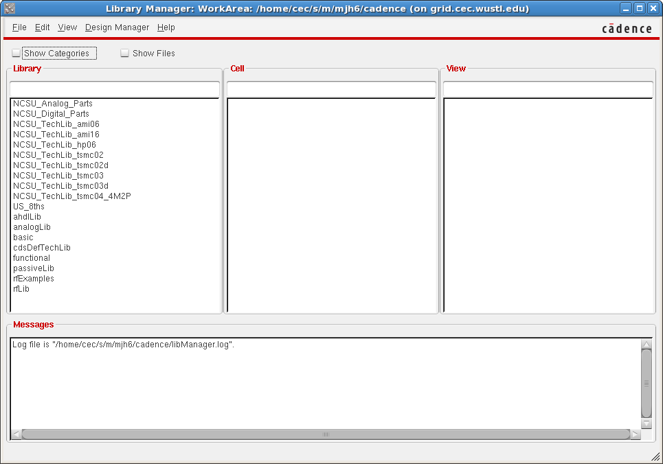
The Library Manager window should appear in just a few moments. This window should be similar to the one below:
The left column is a list of the current libraries. From these libraries NCSU_Analog_Parts is of most importance. This library contains all the components used during VLSI circuit design and it will be used the most.
Left click on NCSU_Analog_Parts in the library browser. Left click on nmos4 to display the cell views of the nmos transistor design. You should be able to see several different cell views. The cell views contain the following information:
| Cell view | Description |
|---|---|
| symbol | Contains the symbol representation of the schematic. |
| CdsSpice, Spectre, spectreS | Contain spice information for the element. Feel free to look at any of the cell views. To do this, click center and hold on the cell view and choose read or you can double click on the particular cell view of interest. A window will open showing the contents of that particular window. In different cells, you may encounter the following cell views: |
| abstract | Contains an abstract representation of the layout for use by Cadence place and route software. |
| extracted | Contains layout connectivity for use by verification programs. |
| layout | Contains the silicon-level representations of the transistors and wiring (you'll do this a lot!). |
| schematic | Contains the logical design of the device. |
| behavioral | Contains the VHDL description of the cell. |
Design Hierarchy
- Library
- Libraries let you organize design data and perform version access and control. A library is a collection of logical design objects, organized in levels as shown:
- Cell
- A cell is the basic design object. It forms an individual building block of a chip or system. It is a logical, rather than physical, design object. Each cell has one or more cell views as shown above. Cells can be logically grouped into cell categories. A cell can belong to several cell categories.
- Cell view
- A cell view is a virtual data file created in association with a cell and a view. It is a logical, rather than physical, design object.
The Cadence software manages these files transparently. However, because of the relationship between cells, you must use the commands copy, move, and delete within the Cadence software in order to manipulate the different cells. UNIX operating system commands cannot correctly handle these files.
Quitting the Session
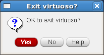
Left click CIW: File → Exit...
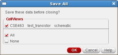
A dialog box should appear, and ask to confirm the request. Left click OK to exit Cadence, or left click Cancel to resume. If you have any unsaved work, the Save All form appears with the library, cell, and cell view names.
Left click on OK after making all the appropriate choices. All Cadence windows will now close, and the design session will end.
Creating a new library
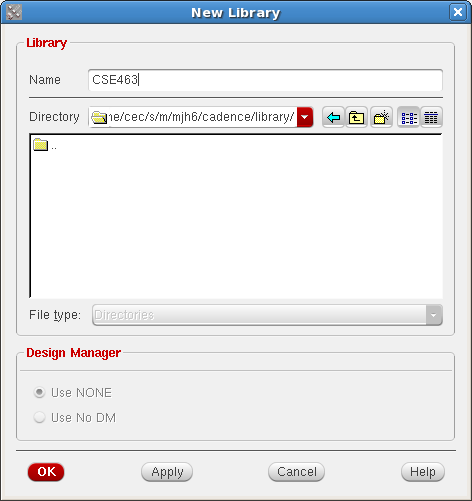
Start the Cadence software and the Library Manager will automatically pop up. In the Library Manager click on: File → New → Library.
A dialog box should appear and you should fill the appropriate boxes as shown in the picture below. Note: you should store your new libraries in a separate directory. In this example, create a directory named "library" under your cadence directory as shown in the figure below:
Press the OK button. You can choose any name for the library. In this case we have chosen CSE463 for the library name. Cadence will automatically create a subdirectory named CSE463.
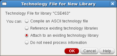
Next you will see the Technology File for New Library window. This window allows you to specify the technology you will use for your IC design. For our class, we will use AMI 0.6micron technology. Select the option shown in the figure below:
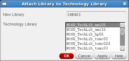
Press the OK button. The Attach Library to Technology Library will appear. Select the NCSU_TechLib_ami06 option and press OK.
A new library named CSE463 has been created in the directory that was specified above. This step is performed only once. In this library, new cells will be designed such as inverters, nand, nor, etc.
Creating Schematic for Transistor Testing
Click Library Manager: New → Cell View...
The New File form should appear as shown below. We will be making a test transistor schematic, so type test_transistor in the Cell field. In the View field type schematic or from the Type pull-down menu choose schematic and the View field will be automatically filled. In the Application section, select the following: Open with Schematic XL and check the box next to Always use this application for this type of file. Once you make these two selections, in the future they will be automatically selected.
Left click the OK button.
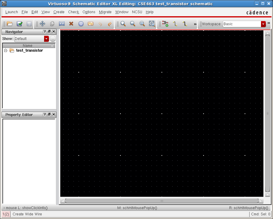
The Virtuoso Schematic Editor window should be showing on your screen as shown in the figure below:
Left click: Schematic Editor: Create → Instance... (bind key <i>)
Shortcuts: You may notice letters by some of these menu choices. Rather than clicking through all the menus, you can just hit that button on the keyboard to the same effect. These are called bind-keys. In the future, you can press <i> in order to insert an instance.
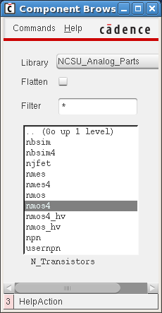
A Command Browser window appears. In this window, select NCSU_Analog_parts under Library pull down menu. Next click on N_Transistors → nmos4. The window should look as shown in the figure below:
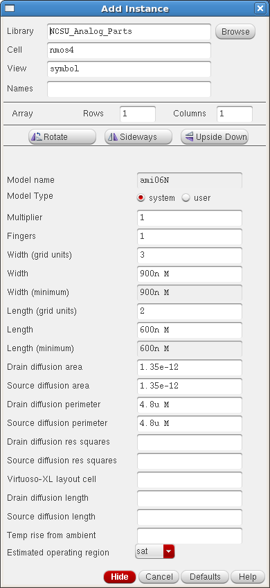
Once you select nmos4, an Add Instance window appears. Type nmos4 to choose a four terminal NMOS transistor in the Cell box and symbol in the View box. Note that you can use the Browse button in order to browse through the libraries and find the cell you want. You can edit the parameters of the nmos4 cell, such as width, length, etc. For this exercise, keep the default parameters. The Add Instance window is shown in the figure below.
Move the cursor into the editing window. Notice that there is a NMOS transistor there instead of the normal cursor. Position it where you want to put the transistor, and left click to place it. You can right click to rotate the transistor if you want it to face a different direction (this is especially useful with pins). While placing, moving, stretching, etc., you can press F3 to show the options form for the command if it is currently hidden.
Press <Esc> to return to a normal cursor after you have finished placing all the transistors you want. For this inverter example, place it on the bottom half of the screen on the right side of the center-line. To rotate press <r>.
To make life easier: Before trying to place a component, left click the Hide button on the Add Component window. This will move it into the background so it's out of your way.
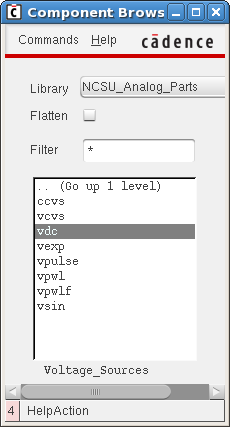
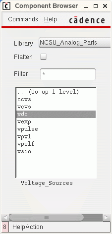
Now we want to add voltage DC sources. Left Click Schematic Editor: Create → Instance.... In NCSU_Analog_Parts library, under Voltage_Sources category, you will find the vdc source. Place it in the test circuit. The Component Browser should look like the one below:
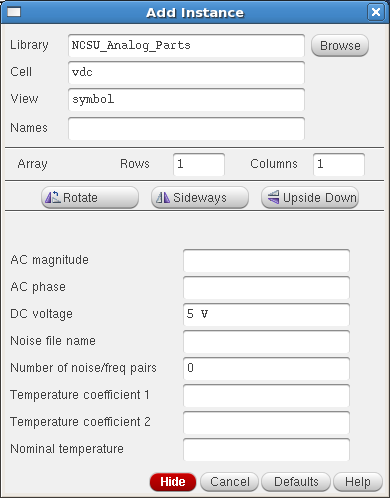
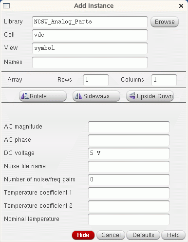
Select Vdc. The Add Instance window will appear. In the DC Voltage field enter 5V (note, the "V" is automatically added when you tab off of the field). This window should appear as such:
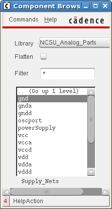
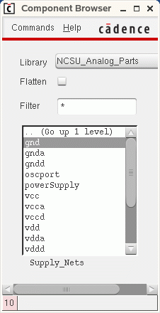
Place the symbol to the left of the transistor. Now we want to add ground lines. Left click Schematic Editor: Create → Instance.... In NCSU_Analog_Parts library, under Supply_Nets category, you will find gnd symbol. Place it in the test circuit. The Component Browser should look like the one below.
Once you select the gnd symbol, the Add Instance window for gnd should look like the one below:
Now, we'll add all the wires to make the circuit work. Left click Schematic Editor: Create → Wire (bind key <w>). The Add Wire form should appear. Just click its Hide button. You can refer to the figure below to see how everything is connected together.
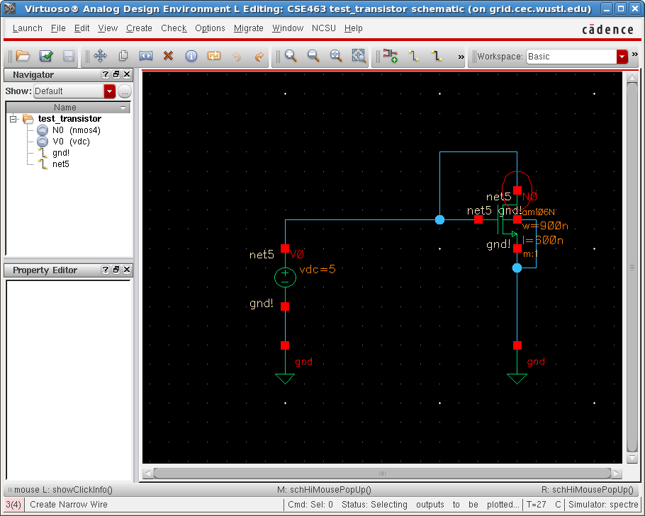
Notice that as you get closer to one pin than another (including those on devices), a small diamond will show up inside of or around that pin. That is where you want to click to connect a wire. Also, when wiring the schematic, leave the wire width at 0, Route method at full, and (usually) Draw Mode as route. This tells the software to auto-route the wires for you. If you put a wire where you don't want it to go, you can delete the wire by left clicking Schematic Editor: Edit → Delete (bind key <del>) and then left click on the object you want to delete (wire, pin, component, etc.).
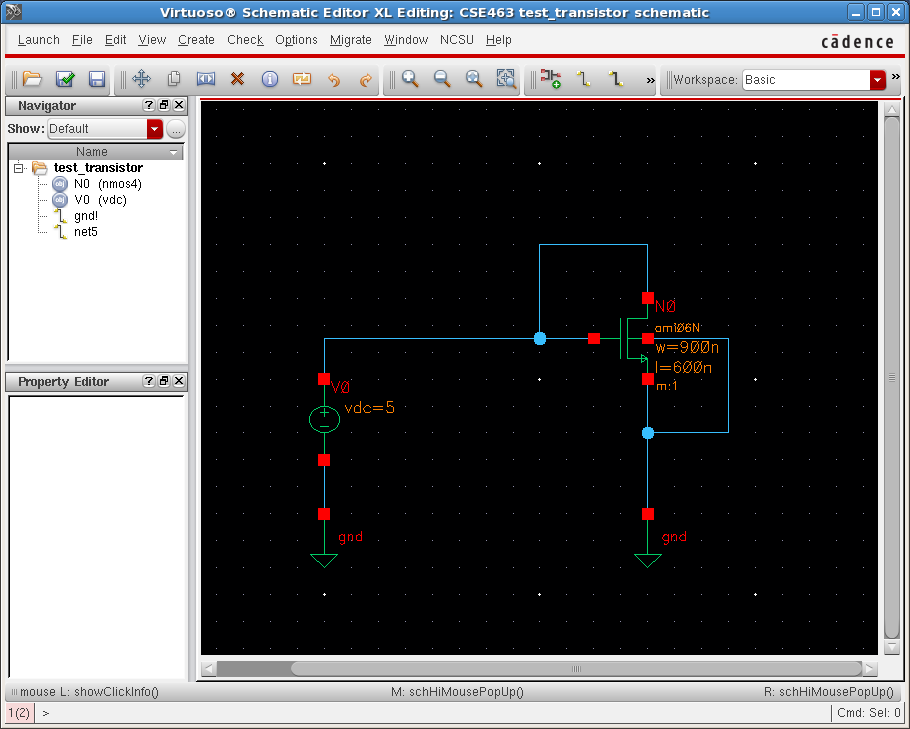
A picture of what the circuit should look like is shown below:
Once you are done editing, left click the "check mark" icon on the left side of the screen. This will check your work for connection errors and will save your work in the library. You can accomplish the same thing by left clicking Schematic Editor: File → Check and Save.
Schematic Simulation of Test Transistor
In the schematic of test_transistor, left click Schematic Editor: Launch → ADE L. The Spectre window should appear.
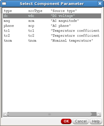
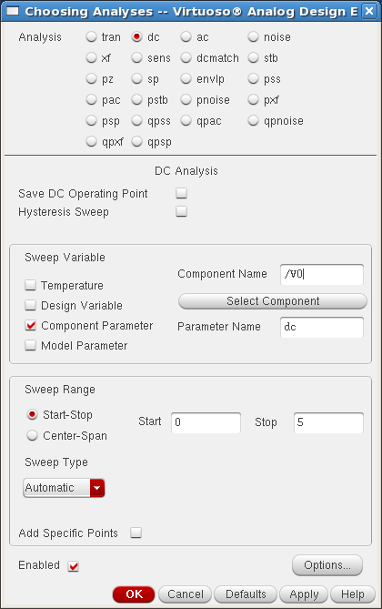
We want to specify the type of analysis we want to perform. We are going to select a DC analysis. Left click Analog Artist: Analyses → Choose.... Click on the dc button for Analysis. Left click Component Parameter button for under Sweep Variable. In the Sweep Range, fill 0 and 5V for the Start and Stop. Left click on the Select Component. Now go back to the schematic and select the voltage source you want to sweep. Click on the vdc that is connected to the input of the inverter. This will pop-up the Select Component Parameter form shown below, which requests the selection for the Parameter Name.
Left click on dc to sweep the voltage and then click OK to go back to your Analysis Choose window, which should look like the one below.
Left click OK.
Second, we want to select which output voltages to be plotted. Left click on Analog Artist: Outputs → To Be Plotted → Select On Schematic. We want to plot the drain-source current of the transistor. Click on the square of a symbol where the current is flowing through (in this example, the square of the drain terminal of the transistor symbol). There will be a circle around the square node indicating that a current is selected. Once you have selected the current to be plotted, the schematic will look as follows:
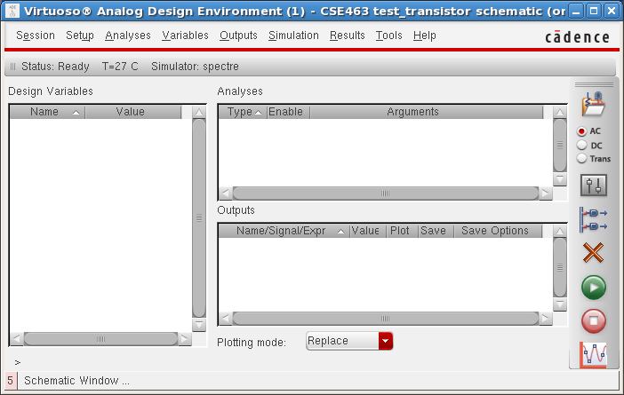
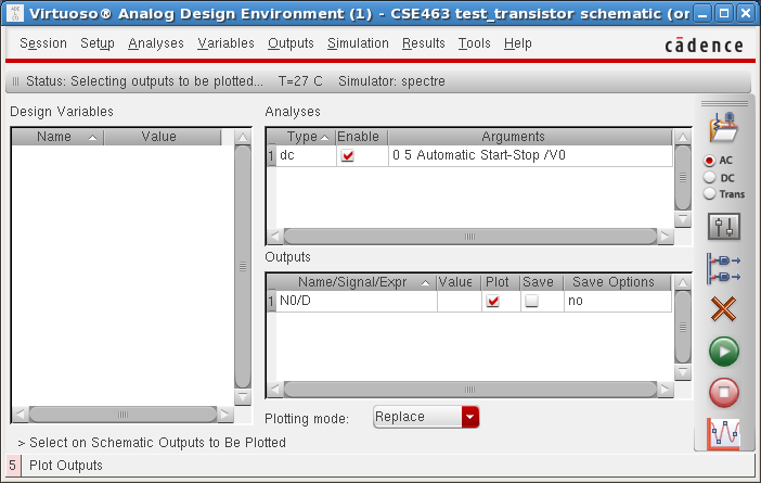
Your Analog Design Environment window should appear similar to the figure below:
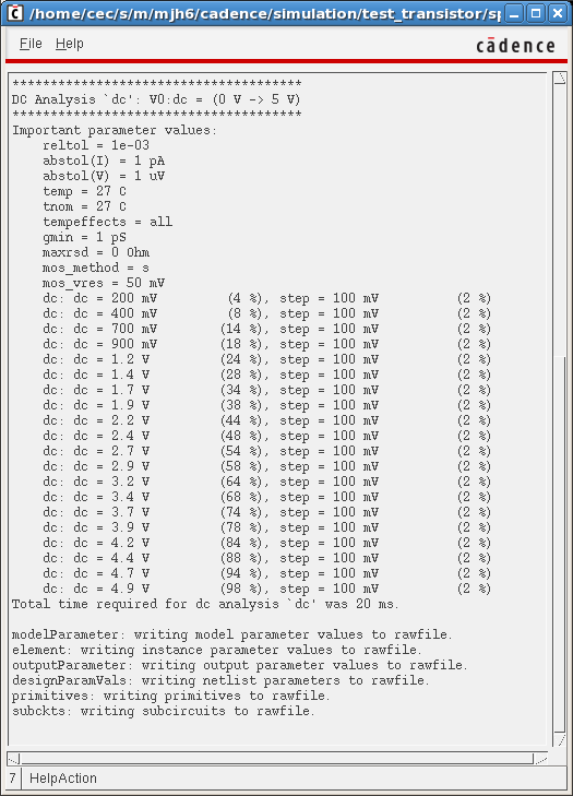
You are ready to run the simulation. Left click Simulation → Run or click on the green play icon in the Analog Design Environment window. The Spectre output window appears as shown below, followed immediately by the Waveform window:
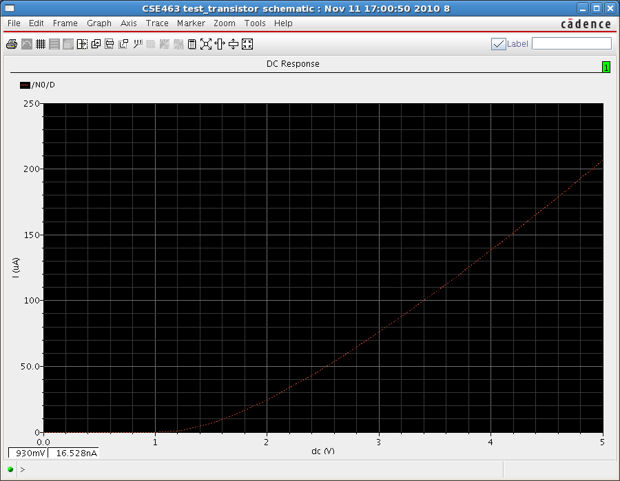
The results appear in the Waveform window, as shown below:
Explore the pull down menus in this window in order to customize your results. For instance, left click Axes → Strip in order to separate multiple curves (you must have more than one output selected for plotting for this to be available). Press on the calculator icon. This icon will bring up a calculator and you can perform various operations on the output waveform, such as derivatives, square root, max, min, etc.
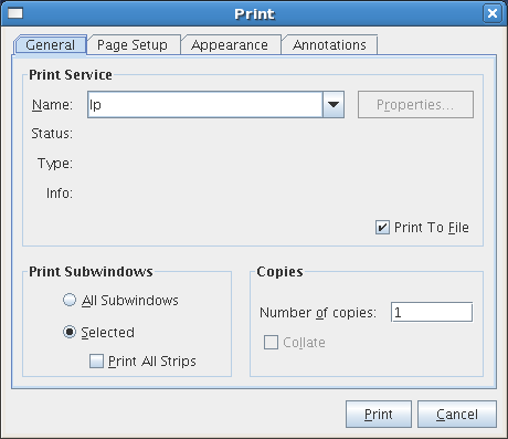
To plot the results left click Waveform Window: File → Print.
Select the option to Print To File to save it as Post Script. Left click Print.
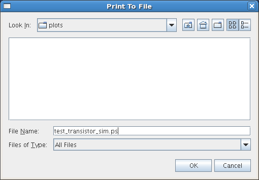
Create a directory named plots. Then type a name for the Post Script file and left click OK. A plot of the waveform is now created. Note, this can be converted to PDF using the UNIX command ps2pdf.
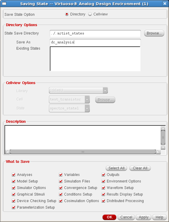
Now exit the Cadence Spice. Left click on Analog Artist: Session → Quit. Cadence will ask whether or not you want to save the current state as shown below:
If you choose Yes to save the current state, the Saving State form will appear:
Type a name for the state in the Save As field and left click OK.
Creating a New Cell: Inverter
Click Library Manager: New → Cell View...
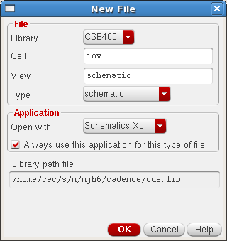
The New File form should appear as shown below. We will be making an inverter, so type inv in the Cell field. In the View field type schematic or from the Type pull-down menu choose schematic and the View field will be automatically filled. In the Application section, select the following: Open with Schematic XL and check the box next to Always use this application for this type of file. Once you make these two selections, in the future they will be automatically selected.
Left click the OK button.
The Virtuoso Schematic Editor window should be showing on your screen as shown in the figure below:
Left click: Schematic Editor: Create → Instance... (bind key <i>)
Shortcuts: You may notice letters by some of these menu choices. Rather than clicking through all the menus, you can just hit that button on the keyboard to the same effect. These are called bind-keys. In the future, you can press <i> in order to insert an instance.
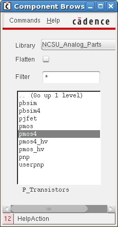
A Command Browser window appears. In this window, select NCSU_Analog_parts under Library pull down menu. Next click on P_Transistors → pmos4. The window should look as shown in the figure below.
Type pmos4 to choose a four terminal PMOS transistor in the Cell box and symbol in the View box. Note that you can use the Browse button in order to browse through the libraries and find the cell you want. You can edit the parameters of the pmos4 cell, such as width, length, etc. For this exercise, keep the default parameters. The Add Instance window is shown in the figure below.
Move the cursor into the editing window. Notice that there is an PMOS transistor there instead of the normal cursor. Position it where you want to put the transistor, and left click to place it. You can right click to rotate the transistor if you want it to face a different direction (this is especially useful with pins). While placing, stretching, etc., you can press F3 to show the options form for the command if it is currently hidden.
Press <Esc> to return to a normal cursor after you have finished placing all the transistors you want. For this inverter example, place it on the bottom half of the screen on the right side of the center-line. To rotate press <r>.
Click Schematic Editor: Create → Instance...
Follow the same steps as before, but choose a nmos4 transistor. Use the default values for length and width. Place the NMOS transistor somewhere below the PMOS transistor.
To make life easier: Before trying to place a component, left click the Hide button on the Add Component window. This will move it into the background so it's out of your way.
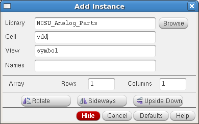
Repeat the same procedure as above and add both gnd and vdd symbols. Place the gnd symbol below the nmos4 transistor and place the vdd symbol above the pmos4 transistor. Refer to the final figure at the end of this section to see the placement of all components. When adding the gnd and vdd symbols, the Add Instance window appears and it should look like the ones shown below.
Now, we'll add the pins for the inverter. Click Schematic Editor: Create → Pin (bind key <p>).
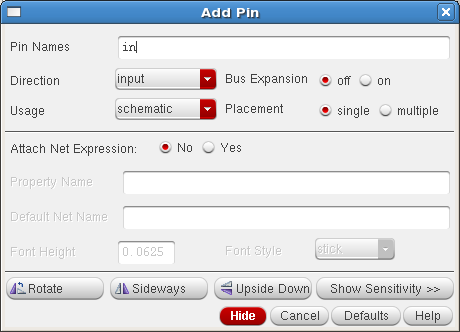
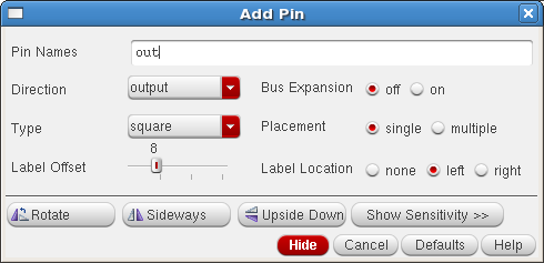
The Add Pin dialog box comes up. In the Pin Names field enter the pin name in (note, multiple pin names can be given, separated by a space) and ensure that Direction is set to input. The Add Pin window should look as follows:
Place the in pin somewhere towards the left side of the editing window, between the two transistors.
Click Schematic Editor: Create → Pin again. The Add Pin dialog box comes up. In the Pin Names field enter the pin name out and ensure that Direction is set to output. The Add Pin window should look as follows:
Place the out pin somewhere towards the right side of the editing window, between the two transistors.
Now, we'll add all the wires to make the inverter work. Click Schematic Editor: Create → Wire (bind key <w>). The Add Wire form should appear. Just click its Hide button. You can refer to the figure at the end of this section to see how everything is connected together.
Notice that as you get closer to one pin than another (including those on devices), a small diamond will show up inside of or around that pin. That is where you want to click to connect a wire. Also, when wiring the schematic, leave the wire width at 0, Route method at full, and (usually) Draw Mode as route. This tells the software to auto-route the wires for you.
If you put a wire where you don't want it to go, you can delete the wire by left clicking Schematic Editor: Edit → Delete (bind key <del>) and then left click on the object you want to delete (wire, pin, component, etc.).
Make all of the following wire connections:
- Gates - For the first wire, left click on the gate terminal of the pmos4 transistor, and left click again on the gate terminal of the nmos4 transistor. You have just connected the gates.
- Input - Now, move the mouse until the little square is inside the diamond on the in pin. Left click in the diamond. Move the cursor over to the wire you connected the two gates together with. A diamond will form around the cursor, as long as it's on the wire. Left click on the wire. You have just connected the input to the gates of both transistors.
- Body - The body of the nmos4 and pmos4 transistors are the center pins. On the pmos4 transistor, connect this pin to vdd. On the nmos4 transistor, connect the body to gnd.
- Sources - The source of the nmos4 transistor is the bottom terminal with an arrow pointing out and the source of the pmos4 transistor is the top terminal with an arrow pointing in. Connect the source of the nmos4 transistor to gnd and the source of the pmos4 transistor to vdd.
- Drains - There should now only be one pin left on each transistor (the drains of both transistors). Connect these two pins together.
- Output - Finally, connect the drains wire to the out pin.
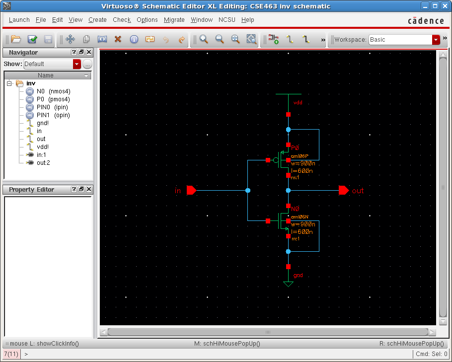
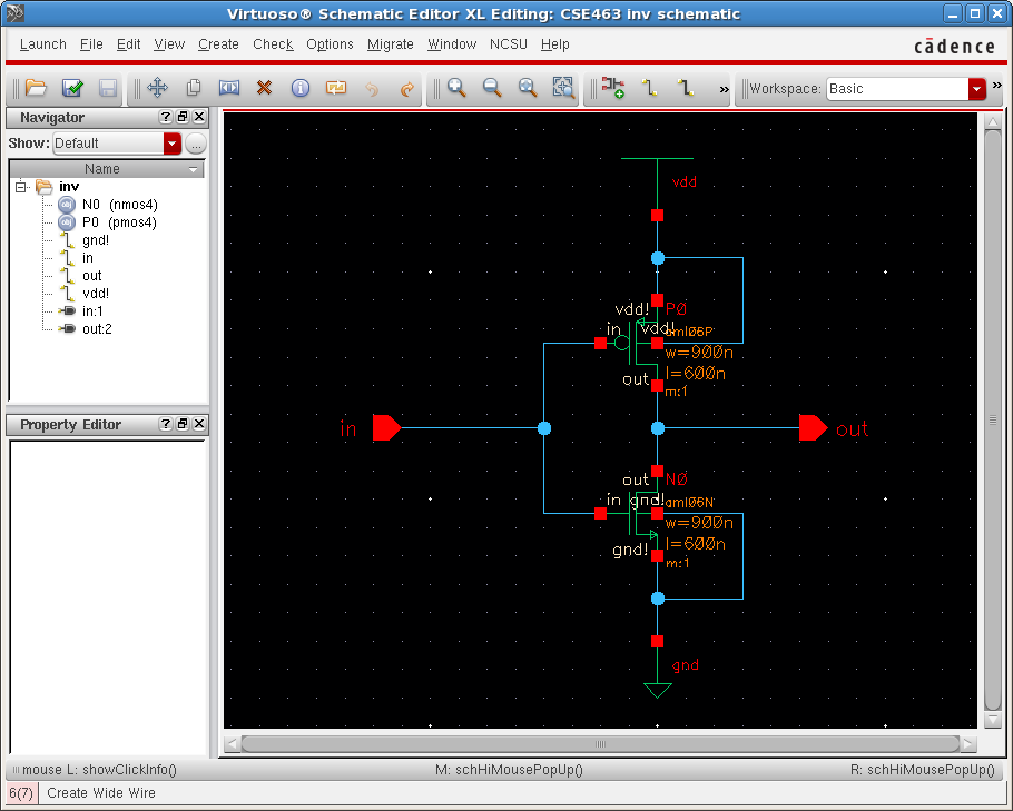
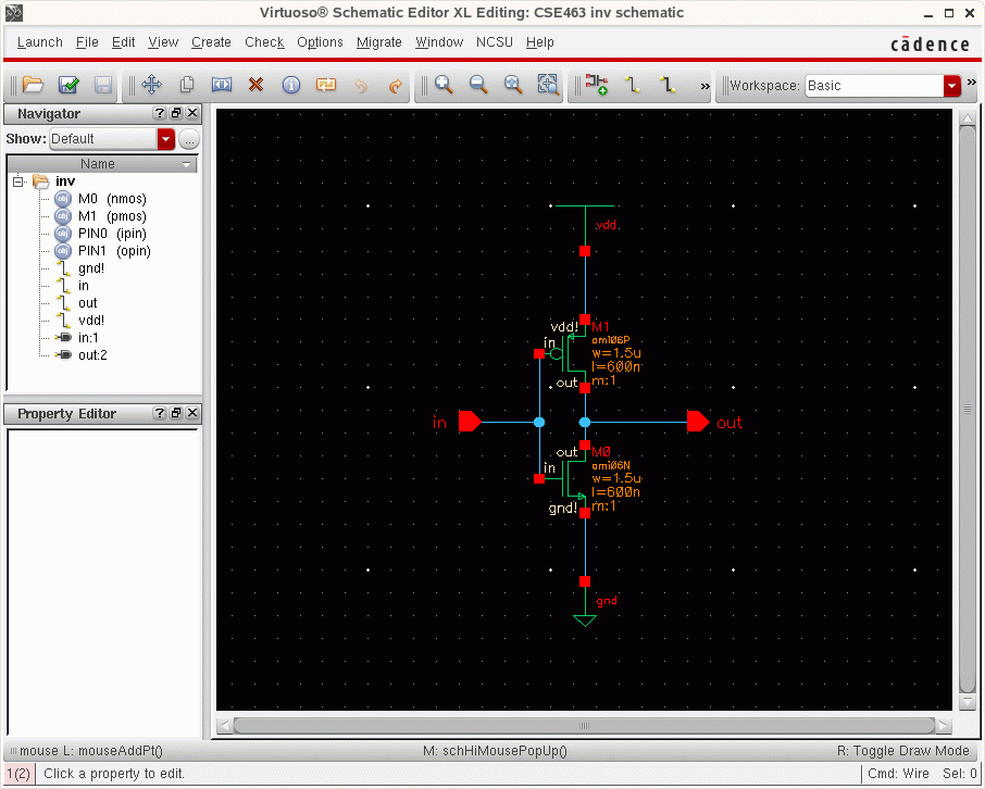
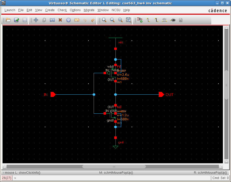
A picture of what this should all look like is shown below:
Once you are done editing, left click the "check mark" icon on the left side of the screen. This will check your work for connection errors and will save your work in the library. You can accomplish the same thing by left clicking Schematic Editor: File → Check and Save.
Printing your Schematic
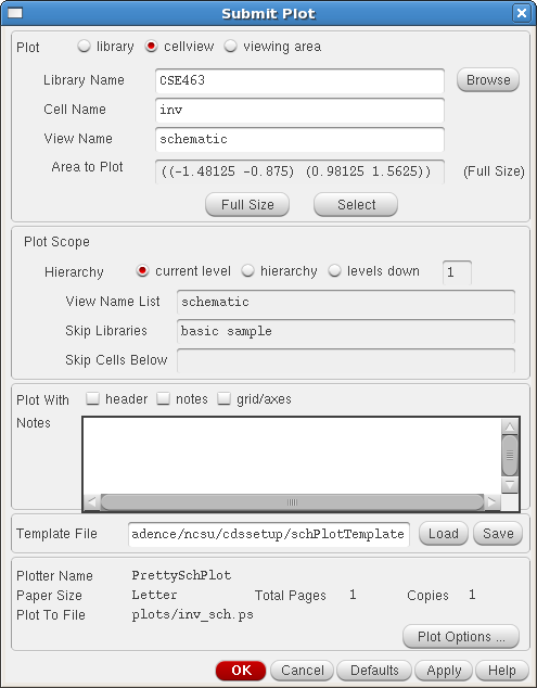
Now that the schematic is complete, you'll want to print it out. To do this, left click Schematic Editor: File → Print. The Submit Plot window should appear.
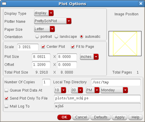
Make sure that the "header" check box next to Plot With is NOT selected in the Submit Plot window. The header option will produce an extra page with general information of your plot such as the name of the plot, size and etc. Left click in the Plot Options button. The Plot Options window will appear.
Check the "Send Plot Only To File" and type in a descriptive name about the plot. Be sure to end the name with the ".ps" extension, as seen above. What you are plotting is a PostScript file. Left click OK in the Plot Options window and also in the Submit Plot window. When the machine is done creating the file, it will send you mail telling you that it completed successfully. To prevent this, you can uncheck "Mail Log To". You can now use the print tool to plot your schematic.
Note: You can modify your PostScript file by using the GIMP program installed on Linux machines. This is not the only way to do it. There are other different ways to modify .ps files.
Creating Symbols: Inverter Symbol
The symbol editor lets you create a "black box" description of a cell using labels, pins, shapes, notes, and a selection box. Symbols make your design more readable, as you can use them in more complex designs, instead of individual transistors.
There are two different ways you can create a symbol: create a new symbol cell view using the Library Manager, or generate a symbol cell view from the schematic. Both of these ways are explained in the sub-sections below:
Create a blank symbol cell view
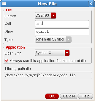
In the Library Manager click once on the CSE463 library to select this library. Then left click Library Manager: File → New → Cell View. In the Cell field type inv and in the View field type symbol. You can also click on the Type box and select schematicSymbol and the View field will be automatically filled.
Left click OK.
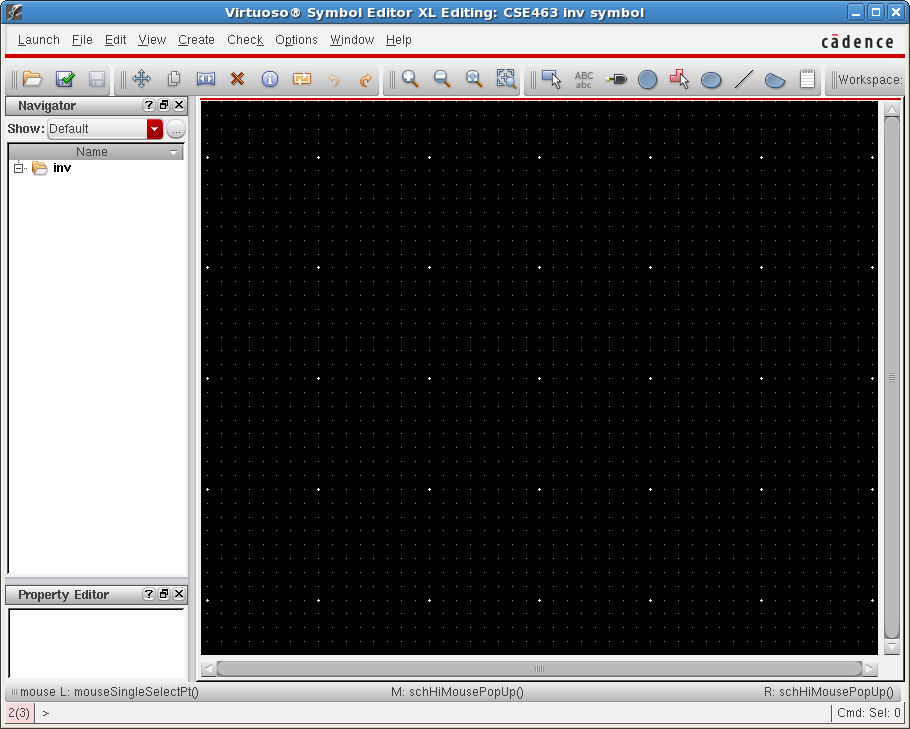
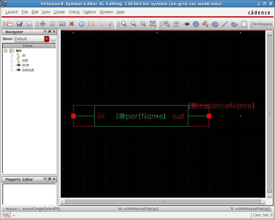
The Virtuoso Symbol Editor window like the one below should appear.
You are ready to draw a symbol for the inverter. First, we will draw a triangle to represent the inverter body. Left click Schematic Editor: Create → Shape → Polygon.
The Add Symbol Shape window appears. Left click Hide for now. To draw a polygon, click at a start point, and then click at the corners of the shape you want to create. To finish the polygon, click again on the start point. Since we are drawing an inverter, we need a sideways triangle, so make one of those. Look at the final picture at the bottom for guidance to draw.
The inverter needs a negation circle at the sideways corner of the triangle, so left click Schematic Editor: Create → Shape → Circle. Hide the Add Symbol Shape window again. Left click at the point you want to be the center of the circle. Move the mouse until the circle is the size you want, and left click again.
Now draw a line that starts at the middle of the vertical line of the triangle and ends somewhere to it's left (about 2 grid line spaces) and another line from the rightmost part of the circle to somewhere equally to the right (again about 2 grid line spaces), so left click Schematic Editor: Create → Shape → Line.
Hint: Rather than invoking the Add Symbol Shape box every time and having to go through the menus, you can use the shortcut buttons located at the top of the window.
Now, you want to add pins to the symbol. Left click Schematic Editor: Create → Pin (bindkey <p>).
In the Pin Names box type the following pin names: in. Change the direction of the pins to input for in and output for out. Also set the Type to square, and the Label Offset to 8.
You are going to start placing the pins in the symbol. The pin looks a little different than the ones in the schematic, so be careful. You will notice that it is a box with the pin name label positioned about 2 grid line spacings away. The end of the line will have the pin name. The box is the actual pin, so it must point AWAY from the rest of the symbol.
Add the in pin on the left of the symbol. The pins in ALL cell views of a single cell must have the same attributes and names. In other words, if the type of the pin is input in the schematic, it should be input type in the symbol also. When you save your symbol, any differences between the pins of the symbol and the pins of the schematic will be reported as warnings. Following these warnings you can figure out where the inconsistency in the design has occurred.
Repeat the same procedure for the out pin. The Add Pin selection box should look like the one below:
Add the out pin on the right of the symbol.
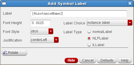
Once you place the pins, the pin names may be hard to read for a variety of reasons. You can therefore move the pin name by clicking on the pin text label and then left click on Schematic Editor: Edit → Move (bindkey <m>). Now you can move the label and place where ever you want to. Next we want to add a label to the symbol. Left click Schematic Editor: Create → Label (bindkey <L>). The Add Symbol Label dialog box should appear.
We will add an instance label. Make sure the Label Choice is set to "instance label" and change the Justification to "centerLeft". Then left click the Hide button, and place the label somewhere near the symbol of the inverter.
Later, when you use symbols to build schematic, the software needs to know which symbol is which. It does this by looking at the instance label to see which one of those it is. If you put multiple symbols into a schematic window, they will be labeled U1, U2, etc.
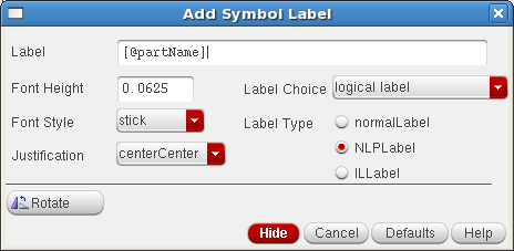
Next, we will add a logical label to the symbol which will describe the circuitry. Choose "logical label" for the Label Choice and change the Justification to "centerCenter". In this case, the label will be [@PartName]. This is a placeholder for the logical name of the inverter cell. When the inverter is later instantiated, the symbol will show the inverter cell name, inv, in place of this logical label. The Add Symbol Label window shown in the figure below:
We will add the label in the symbol. Just left click the Hide button, and place the label somewhere near the symbol of the inverter.
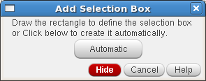
Next, we will add a selection box. This will tell the software how much of the symbol is actually used.
Left click Schematic Editor: Create → Selection Box...
Left click the Automatic button.
Last, we will set the origin point in the symbol. The origin point corresponds to the location of the mouse relative to the symbol when the cell is instantiated. We will set this point to the lower left corner of the selection box. Click Schematic Editor: Edit → Origin. Then left click on the lower left corner of the selection box to set the origin point.
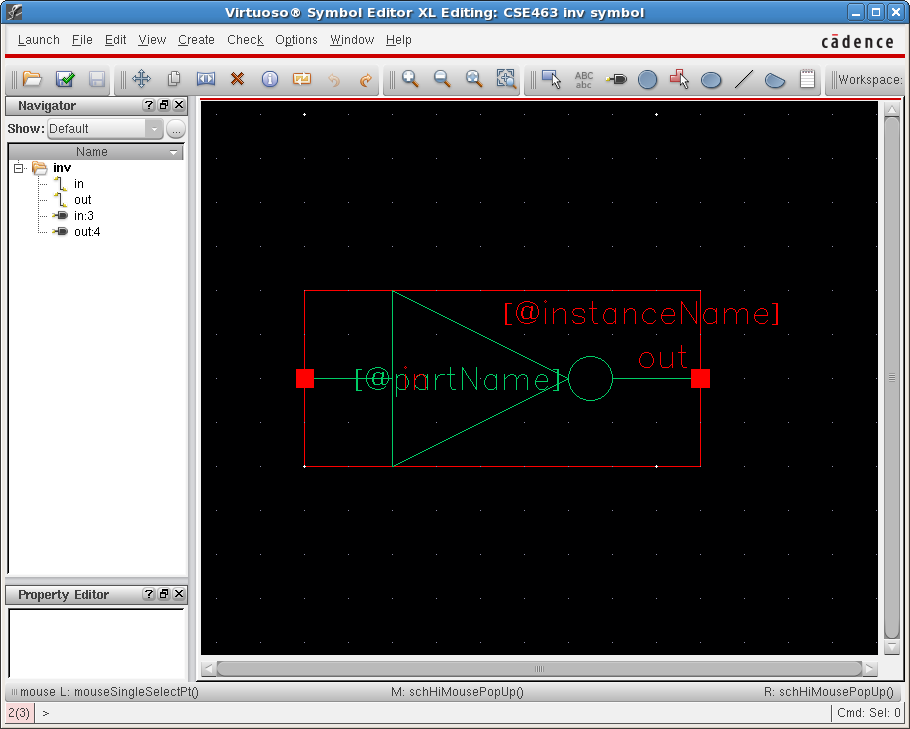
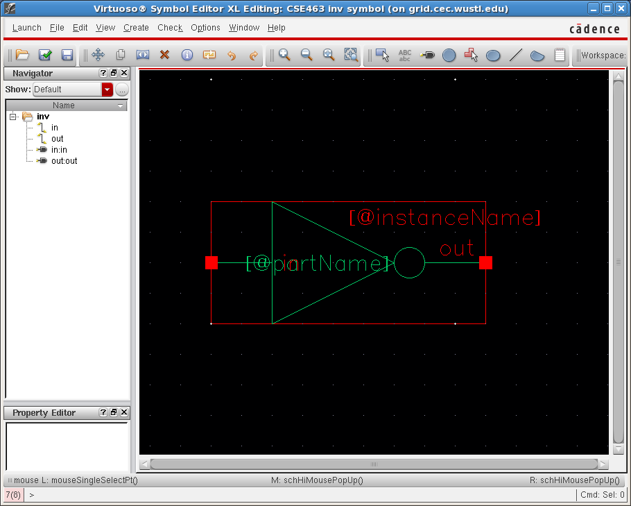
The symbol is now finished and you can save it by left clicking Schematic Editor: File → Check & Save (F8). The symbol should look like the one below.
Generate symbol from schematic
In the Library Manager click once on the CSE463 library to select this library. Then left click the inv cell and finally the schematic cell view. Right click on the schematic cell view and click Open or double click on schematic to open the schematic editor. This will give the figure shown below.
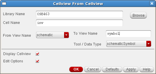
Left click Schematic Editor: Create → Cellview → From Cellview... This will then show the Cellview From Cellview window below. This window allows a symbol to be generated from the schematic view. It does this by identifying the pins that are already defined in the schematic and automatically generating a symbol with the same pins.
Click OK.
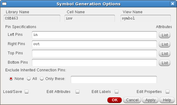
Next, the Symbol Generation Options window will appear which will list the pin specifications of the new symbol. Cadence has already identified the input and output pins and has automatically added the input pin, in, to the left pins and the output pin, out, to the right pins. The Symbol Generation Options window is shown below.
Click OK.
Cadence has now generated a default symbol using the pin specifications previously given. You can now use this symbol as a starting point to create the inverter symbol.
First, we will draw a triangle to represent the inverter body. Left click Schematic Editor: Create → Shape → Polygon.
The Add Symbol Shape window appears. Left click Hide for now. To draw a polygon, click at a start point, and then click at the corners of the shape you want to create. To finish the polygon, click again on the start point. Since we are drawing an inverter, we need a sideways triangle, so make one of those. Look at the final picture at the bottom for guidance to draw.
The inverter needs a negation circle at the sideways corner of the triangle, so left click Schematic Editor: Create → Shape → Circle. Hide the Add Symbol Shape window again. Left click at the point you want to be the center of the circle. Move the mouse until the circle is the size you want, and left click again.
Hint: Rather than invoking the Add Symbol Shape box every time and having to go through the menus, you can use the shortcut buttons located at the top of the window.
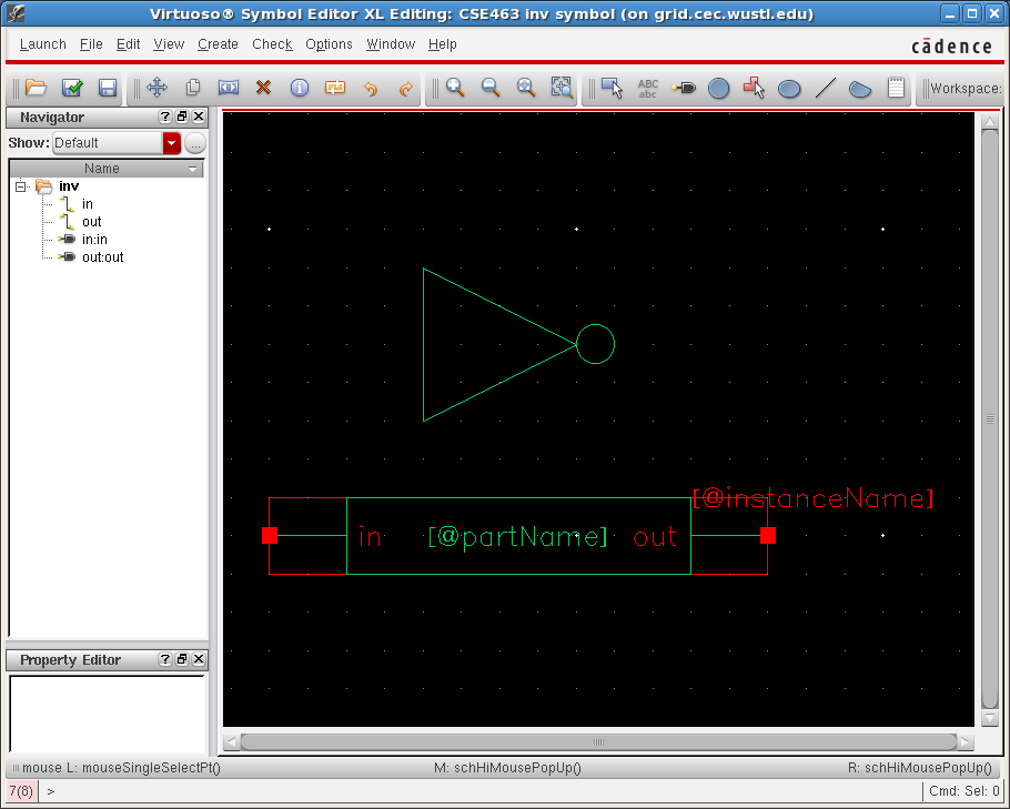
You should have a symbol that currently looks like the one below:
Next, you can move the each pin (along with the line connected to each pin) from the default symbol to the inverter symbol. Left click on Schematic Editor: Edit → Move (bindkey <m>). Now you can move the in pin to the left of the inverter symbol and the out pin to the right of the inverter symbol. You may also want to move the pin name labels to more suitable locations as necessary so that they are easy to see.
Next, move the [@instanceName] label from the default symbol to the inverter symbol positioned to the upper right (note, this label is by default centerLeft justified). Also move the [@partName] label and position it in the center of the inverter (note, this label is by default centerCenter justified). Last, move the red selection box to the inverter symbol. The selection box will need to be resized so that it fits around the inverter symbol. This is done by left clicking Schematic Editor: Edit → Stretch (bindkey <s>). The selection box will tell the software how much of the symbol is actually used.
Now, delete the rest of the default symbol by left clicking Schematic Editor: Edit → Delete (bindkey <del>) and clicking on the objects to delete.
Last, we will set the origin point in the symbol. The origin point corresponds to the location of the mouse relative to the symbol when the cell is instantiated. We will set this point to the lower left corner of the selection box. Click Schematic Editor: Edit → Origin. Then left click on the lower left corner of the selection box to set the origin point.
The symbol is now finished and you can save it by left clicking Schematic Editor: File → Check & Save (F8). The symbol should look like the one below.
Schematic Simulation: Creating a Test File for Simulating an Inverter
Now that we have built an inverter, we need to simulate it to show that our design is valid. First we need to create a new cell in our CSE463library for testing the inverter. In the Library Manager, highlight the test library and left click on Library Manager:File → New → Cell View.
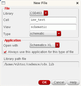
In the Cell Name type inv_test and in the View Name type schematic. Left click on OK.
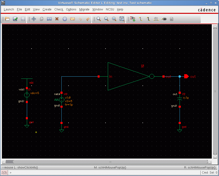
A new schematic editing tool will appear. You are going to instance the inverter that was previously created and connect its input pin to voltage source. The output pin will be connected to a capacitor.
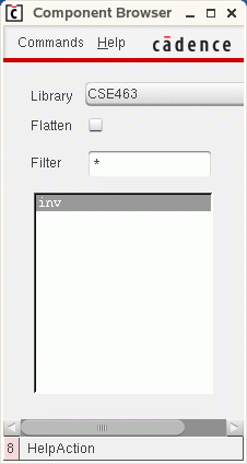
Left click Editing:Add->Instance. Click on the Library pull down menu and select the CSE463 library. Select the inv cell. The Component Browser window should look like the one bellow.
Place the inverter in the middle of the editing window. Note: you can press F3 key while you have selected the symbol you want to place and the Add Instance window will appear. In this window, you can edit some of the properties of the symbol if applicable.
Now we want to add voltage DC sources. Left Click Editing: Add → Instance. In NCSU_Analog_Parts library; you will find vdc sources. Place them in the test circuit. Left Click Editing:Add → Instance. In NCSU_Analog_Parts library, under Voltage_Sources category, you will find vdc source. Place them in the test circuit. The Component Browser should look like the one below:
Select Vdc and Add Instance window will appear. In the DC Voltage field enter 5V. This window should appear as such:
Place the symbol to the left of the inverter.
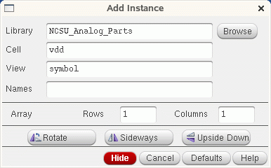
Now we want to add global ground and power lines. Left Click Editing: Add → Instance. In NCSU_Analog_Parts library, under Supply_Nets category, you will find vdd and gnd sources. Place them in the test circuit. The Component Browser should look like the one below.
Once you select the NCSU_Analog_Parts selection and select Supply_Nets, you will find gnd and vdd symbols. The Add Instance windows for vdd and gnd should look like the ones below:
Left Click Hide and place the vdd and gnd symbols on the schematic. Place the vdd above the vdc symbol and gnd bellow the vdc symbol.
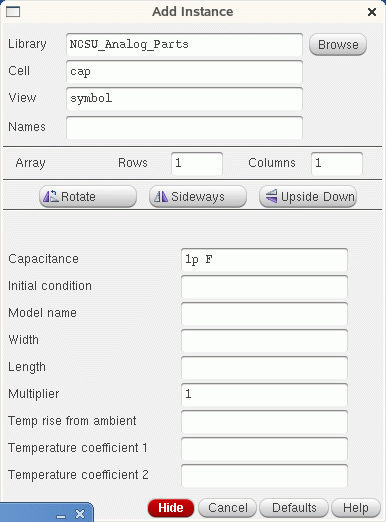
Next, we want to add capacitor to the output pin in order to simulate a load (other circuits) that our inverter has to charge or discharge. Left click Editing:Add → Component. From the NCSU_Analog_Parts library choose a cell named cap and specify its value to be 1 pF. The Add Instance window should look like the one below:
Next we will add an output pin in the schematic. Left click Editing:Add → Pin. Name the pin out and specify it as an output pin. Place the pin next to the output of the inverter.
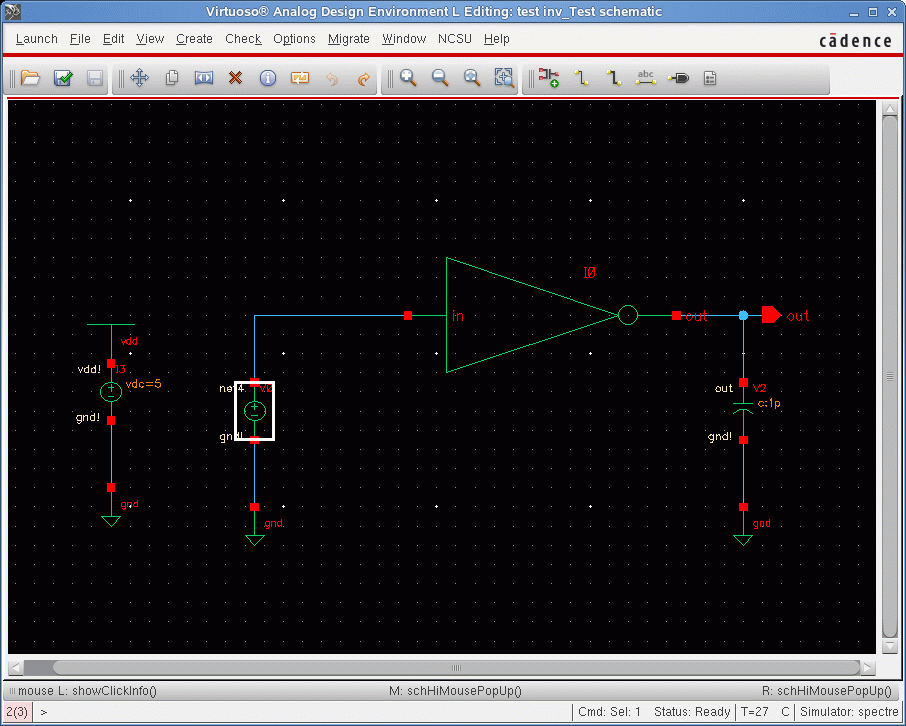
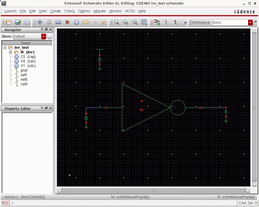
Connect all the elements as shown in the figure below. To connect different elements use Editing:Add → Wire. The final schematic should like the one below:
Save the schematic and you are ready to simulate the inverter.
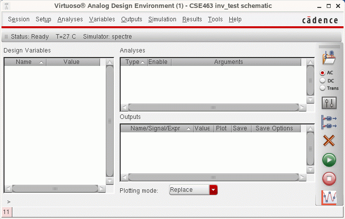
In the schematic of inv_test, left click Editing:Launch → ADE L. The spectre window should appear.
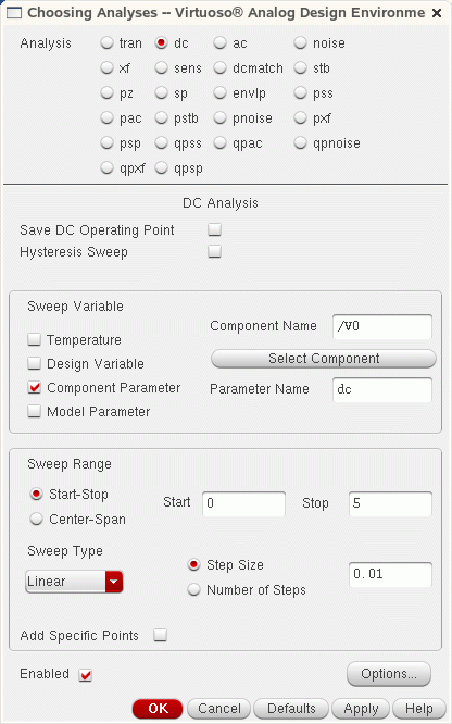
We want to specify the type of analysis we want to perform. We are going to select a DC analysis. Left click Analog Artist:Analyses → Choose? Click on the dc button for Analysis. Click Component Parameter button for sweep variable. In the Sweep Range, fill 0 and 5V for the start and stop. Left click on the Select Component. Now go back to the schematic and select the voltage source you want to sweep. Click on the vdc that is connected to the input of the inverter. This will pop-up a small window, which requests the Parameter Name. Click on dc to sweep the voltage. Go back to your Analysis Choose window, which should look like the one below, and click on OK.
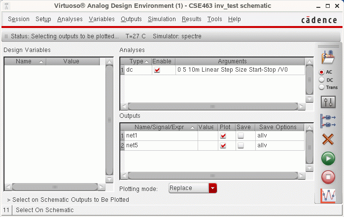
Second, we want to select which output voltages to be plotted. Left click on Analog Artist: Outputs → To be Plotted → Select on Schematic. Click on the wire between your vdc source and the in pin of your inverter. Then click on the wire between the out pin of the inverter and the out pin. Both wires should change color indicating that these voltages will be plotted.
Note: If you want to select a current to be plotted, then click on the square of a symbol where the current is flowing through. There will be a circle around the square node indicating that a current is selected.
Your Analog Environment window should appear similar to:
Note: in order to make your simulation more readable, it is often advisable to name special nets with uniquely identifiable names, so that when the simulation results are presented, they are more easily understood.
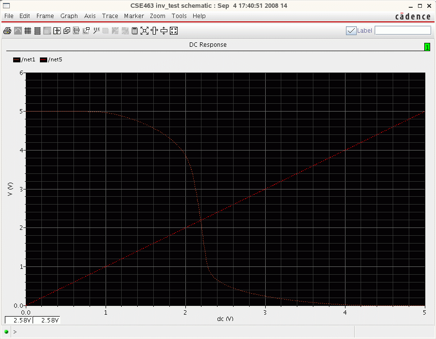
You are ready to run the simulation. Left Click Simulation → Run or click on the green traffic light icon in the Analog Environment window. The result window, as the one below will appear shortly. Explore the pull down menus in this window in order to customize your results. For instance, left click Axes → Strip in order to separate the different curves.
To plot the results left click Waveform Window: Window → hardcopy. Select the option to Send Plot Only to File and also don't forget to disable the header option in order not to waste paper. You might also disable Mail Log To to prevent it from mailing you about the status of printing.
Now exit the Cadence Spice. Left click on Analog Environment:Session → Quit. Remember NOT to save the current state. If you choose to save the current state, several hundreds of megabytes will be used in order to save your last simulation.
Schematic Simulation: Transient Analysis of The Inverter
Bring up the schematic of inv_test. We need to replace the dc voltage input source with a pulse source. Click on the vdc source that is connected to the input of the inverter. The vdc should have a yellow box around it. Go to Editing: Edit → Delete or press the Del button.
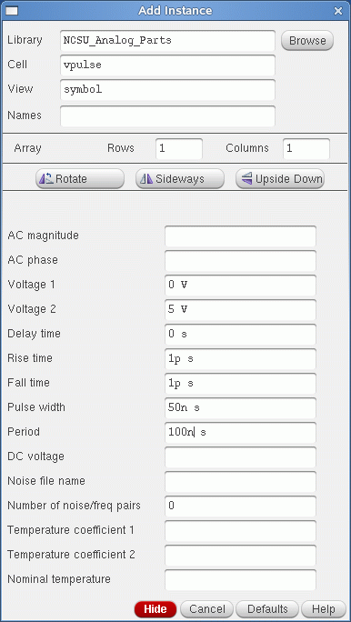
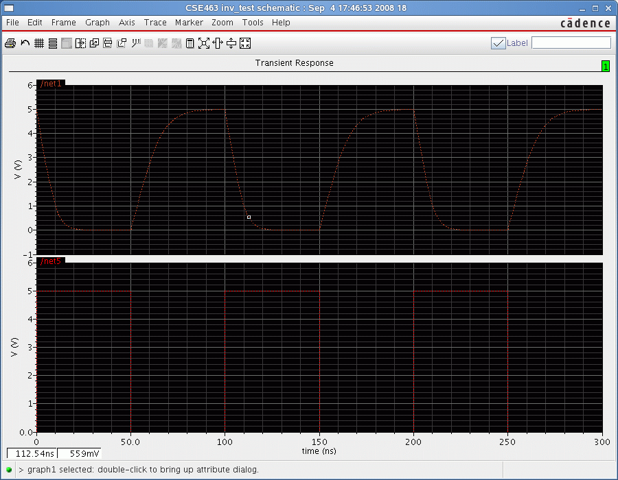
Left Click Add → Instance and select Cell Name: vpulse from Library Name: NCSU_Analog_Parts and View Name:symbol. Fill the rest of the boxes as shown in the figure below. The input pulse that we have specified is bounded between 0 and 5V. It has an initial delay of 1ns, rise and fall time of 1ps and high/low duration of 2ns.
Place this symbol such that the positive end is connected to the input of the inverter.
Save the schematic. Left Click Editing:File → Save. After we have made these changes we are ready to run a transient analysis on the inverter.
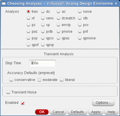
Left Click Editing:Launch → ADE L. In the Analog artist window go to Analysis → Choose... Set the transient analysis with Stop Time as 8n. We have specified a transient analysis from 0 to 300ns.
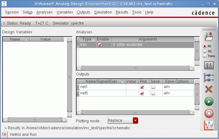
Left Click Analog Artist: Outputs → To be Plotted → Select on Schematic. Select the input and output of the inverter. Refer to the previous section, DC analysis, for the necessary steps. The analogArtist window should look like the one below.
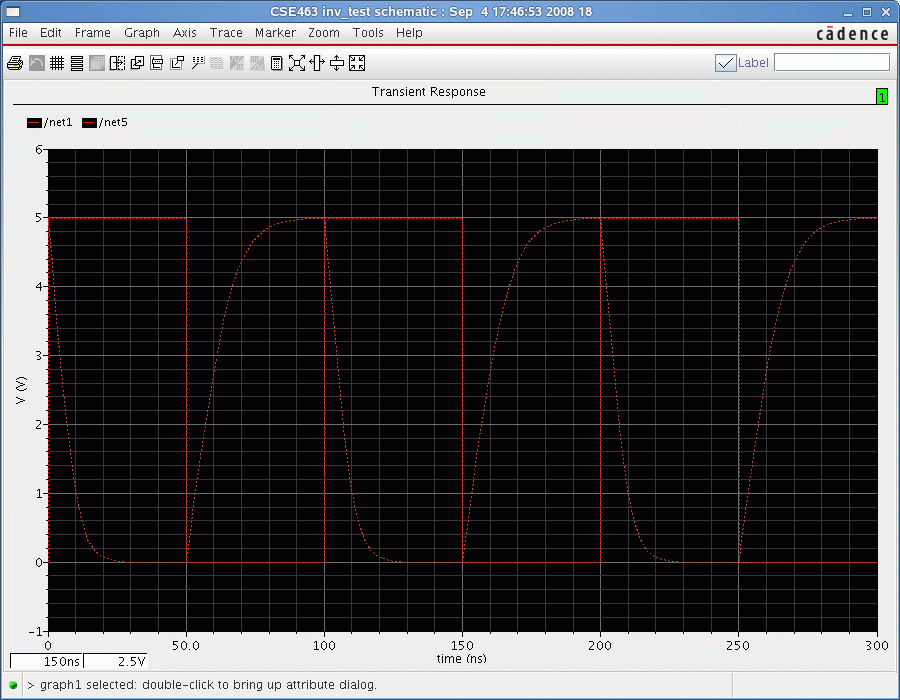
Run the simulation by pressing on the green traffic light icon. After few seconds you should be able to see the results of the transient analyses like the ones below.
Left click Axes → Strip in order to separate the different curves. The result should look like the one bellow:
Parametric Analysis with Spectre
This tutorial will guide you through the process of performing a parametric analysis for the inverter circuit. In particular, we are going to vary the width (W) of the Nmos transistor in the inverter circuit within a specified range and see the effect on the logic threshold value (VLT)
The schematic of the inverter circuit is shown below. I used nmos4 and pmos4 symbols from NCSU Analog library. You can also use your inverter that you designed earlier.
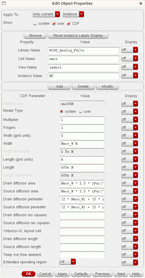
In order to be able to automatically sweep a parameters in a given circuit, this parameter must have a variable name assigned. In our example, the width of the nmos transistor is assigned Nmos_W variable name. This variable name Nmos_W is typed instead of the numeric value which we usually assign, in the nmos property box(shown below).
If other parameters are desired to be analyzed, simply assign a variable name in the appropriate box. Multiple parameters can be also simultaneously parametrically analyzed.
The next step is to create a test schematic for the inverter. You can also use the one that you created before.
Note, that a global assignment for the vdd and gnd are needed. This is done only once, usually at the top level schematic. A Vdc voltage source of 5V is placed between vdd and ground. Once this is declared, all our circuits will be powered from a 5V power supply. Otherwise, Spectre does not know what is the power supply of vdd symbol in your circuit.
Start the Analog Simulator (Launch->ADE L). A new window will appear.
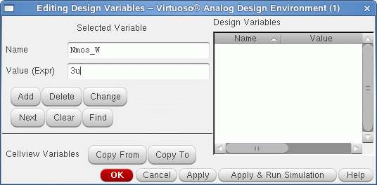
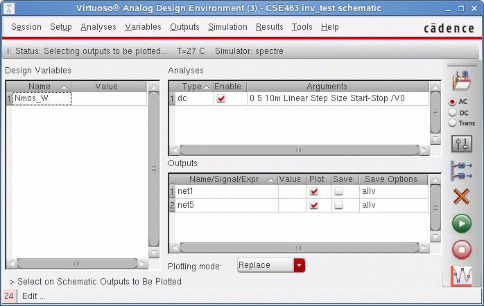
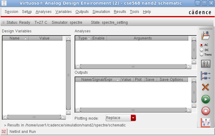
In this window, we will need to specify 3 things. First, the type of schematic analysis. We are interested in a dc analysis and we are going to sweep the V0 voltage source between 0v and 5V. Second, which nets are we going to plotted. We want to plot the input (in) and output (out) nets. And finally, the variable name which we declared earlier must be initialized. If you try to run the simulation without declaring the variable, the simulator will stop and it will enter the variable name in the simulator window automatically. It will then require you to enter a value for this variable. You can also enter yourself the variable name and value. To do so, go in Variables → Edit… in the simulator window. A selection box will prompt you for the name and the value of the variable. Enter the name of the variable and a value and press the add button.
Press OK. Once you have completed these steps, the Virtuoso Analog Design Environment window should look like as below.
The next step is to run the simulation. Press on the "green play" button on the side of the Virtuoso Analog Design Environment window. You should see the following waveform shown below.
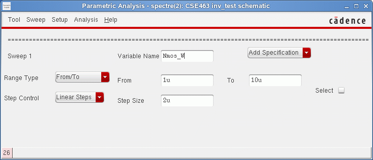
The next step is to perform a parametric sweep analysis of the inverter. We would like to sweep the width of the nmos transistor between 1um and 10um in increments of 2um. To do so, in the Virtuoso Analog Design Environment window go under Tools- >Parametric Analysis. A new window will appear. In this window we will specify the parameters we would like to sweep.
In the Variable Name box, we have entered the name of the variable Nmos_W. In the Range Type section, we have specified a sweep From: 1u To: 10u in Linear Steps increments of 2u. In this window you can add other variables if you want to sweep. You can sweep multiple parameters simultaneously if desired.
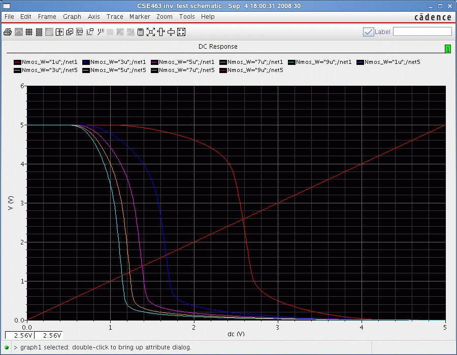
Now you are ready to run the parametric analysis. In the Parametric Analysis window, go under Analysis->Run. This will execute this analysis. The results will be plot after few seconds and they are presented below.
Both input and output waveforms are plotted on the same graph. At the top of the graph, the parameters of the different colors on the graph are explained. You can also point and select a waveform. Once selected, if you hold down the left mouse button and move the selected waveform, a text will appear describing the parameter i.e. Nmos_W value of that particular curve. You can observe that as the width of the nmos transistor is increased the Vlt value i.e. the point where Vin and Vout cross, is moved closer to ground.
Create Custom Layouts
By now, you would have known how to enter and simulate your designs using Spectre. The next step in the process of making an integrated circuit chip is to perform a layout. What is a layout? A layout is basically a drawing of the masks from which your design will be fabricated. Therefore, layout is just as critical as specifying the parameters of your devices because it determines whether yours is a working design or a flop!
There are 2 ways to doing a layout: manual and automated. Manual layout usually enables the designer to pack his devices in a smaller area compared to the automated process but it is more tedious. The automated process, on the other hand, is done using standard cells and usually takes more real estate space but it is much faster. In this tutorial, you will learn how to perform MANUEL LAYOUTS ONLY and a simple inverter layout will be shown. You should know that for the purposes of this course, you are required to know how to design manual layouts, even though Cadence can accommodate either manual or automated layouts.
Before we get into the layout, first you need to understand the design rules for layout. The design rules that we will be using are the MOSIS Scalable CMOS Rules. Design rules gives guidelines for generating layouts. They dictate the spacings between wells, sizes of contacts, minimum spacing between a poly and a metal layer and many other similar rules. Design rules are essential to any successful layout design, since they account for the various allowances that need to be given during actual fabrication and to account for the sizes and the steps involved in generating masks for the final layout. The design rules that we will be using can be obtained from the following link on MOSIS Layout Design Rules. Note that the layout is very much process-dependent, since every process has a certain fixed number of available masks for layout and fabrication. For the case of this tutorial, we are using an AMI 0.6u CMOS process, which is a nwell process and supports two poly and three metal layers.
Before we proceed any further, please make sure that your present library is associated with a techfile. If you had followed this tutorial for your design of an inverter, then you might have already associated a techfile when you created a library ESE570 in the first place. Otherwise, you can still do it, by clicking on the middle button by placing the mouse on the library name in the library manager window. There is an option for "Attach Tech Library". Once you choose that option, click on AMI 0.6u C5N(3M,2P,high-res) as your process.
-
Create a layout cellview of the cell. Here we will create a layout for the inverter cell.
In the library manager window, click on the File → New → CellView. Choose CellName as inverter and View Name as layout. Then click on the OK button. An empty layout editor window will pop-up along with a LSW window. The LSW window will show all the layers such as nwell, pwell, active, etc. for the given process. An alternate way to open the layout editor window is to type "layout" into the View box of the inverter cell in the Library Manager window. A "Create New File" window will pop-up. Change the Tool item from "Composer-Schematic" to "Virtuoso" and make sure the View Name is "layout". If not, manually change this by typing this in.If the LSW window is blank, then there is an error.
The LSW window should look something like this:
If you don't see the above (not necessary to be in the above order) you will need to set the mask layers manually. To do this, go to Edit → Set Valid Layers and select/deselect the masks. Make sure that you at least have the following masks in your LSW window.
nwell, nselect, pselect, nactive, pactive, poly, elec, metal1, metal2, metal3 (all dg's) & metal1, metal2, metal3 (pn's).
-
Since we are using the AMI 0.6u technology, we only have an nwell process to use. Thus, the substrate will be a p-type substrate. We can always assume that the background is a p-subtrate. Now we will create a pmos transistor first. To do that, we need an nwell layer in which the pmos transistor will be formed.
Note: You may adjust the minimum distance between the grids. In order to do it, in the Virtuoso Layout Editing window select Options → Display. A new window will open. On that window, change "Minor Spacing" to a value that you want. In order to work efficiently, you can adjust it to 1 lambda which is 0.3 (it is actually 0.3u but in that window it will be written as 0.3).
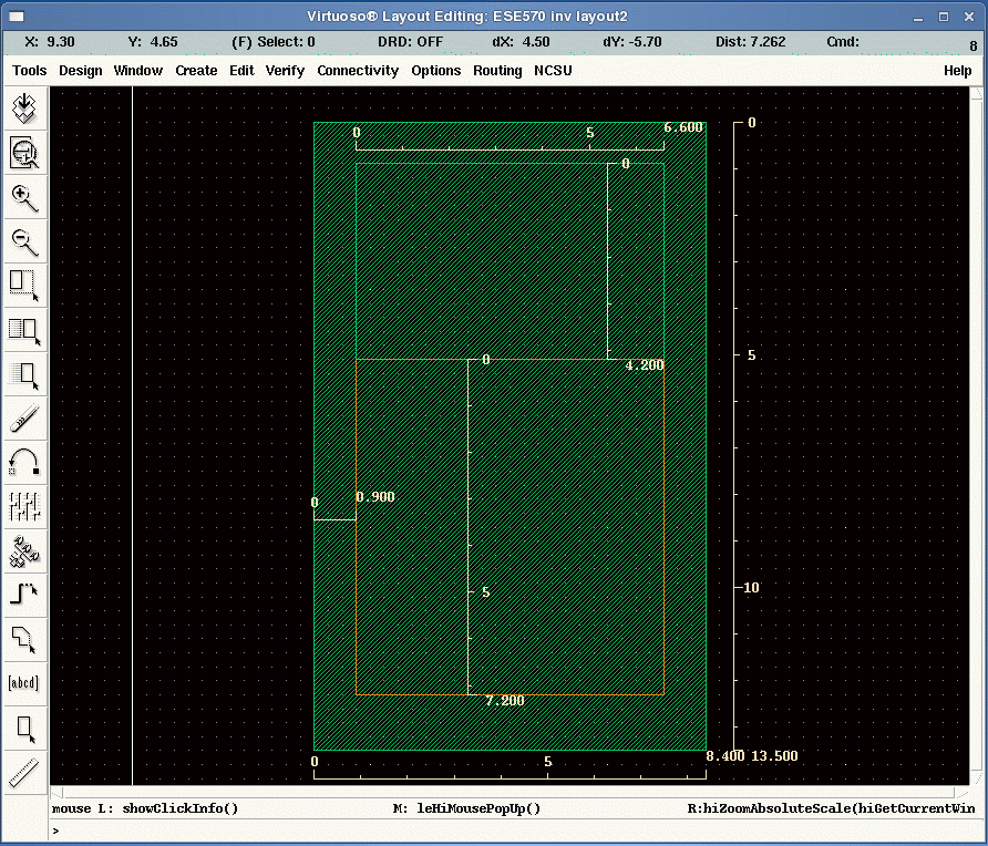
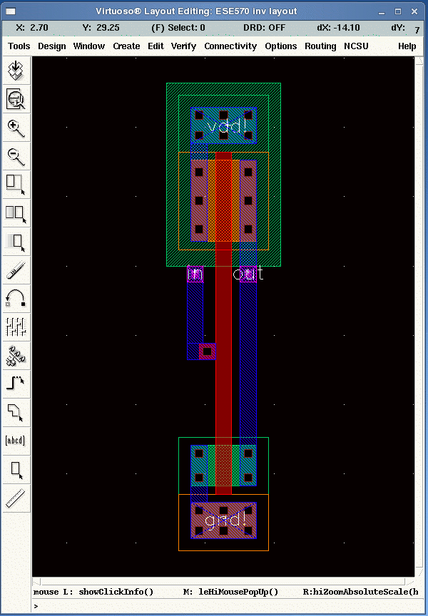
The green-shaded rectangle is the nwell layer, the green perimeter is nselect and the orange perimeter is pselect. The numbers represent the length in um (micrometers). Therefore, for the AMI 1.6u technology, lambda = 0.3u and 2*lambda = 0.6u. The editor options have been defaulted such that every cursor advancement corresponds to 0.15u or 1/4th the 2*lambda feature size. The ruler shown above can be invoked by typing k. It can be removed by typing capital K (shift+k). They show the length in micrometers. Note that you do not have to necessarily follow the dimensions shown above. In fact, it is probably a good idea to play around with the lengths and widths in order to see how small a mask layer you can create without violating any of the design rules.
The LSW window will be used to draw the masks in the layout editor window. To draw a mask, say an nwell layer, first choose the corresponding layer in the LSW window by clicking on the layer. Then, move your cursor into the layout window where you want to draw the nwell layer and type r (rectangle) and move your mouse. A yellow box will appear indicating the boundary of the nwell mask. Just click on the left mouse button to draw the nwell rectangle; we'll worry about the actual dimension later. To change the dimension of the rectangle, move your cursor to the side where you want to extend or shorten such that the side is highlighted and then type s (stretch). The side will move with your cursor.
Likewise, draw the nselect and pselect layers as shown in the figure above.
-
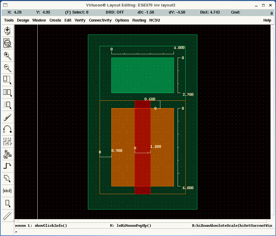
The pselect is where you are creating the pmos transistor since this is where the p+ diffusion is going to be formed. Draw the pactive layer on your layout as shown in the figure below. The orange shaded rectangle is the p+ active regions. The green shaded rectangle is the n+ active region. Next, draw the poly layer to form the gate of the transistor. The size of the pmos transistor shown below has W=6um and L=1.2um using the 0.6um CMOS technology (since 1 lambda is 0.3um).
-
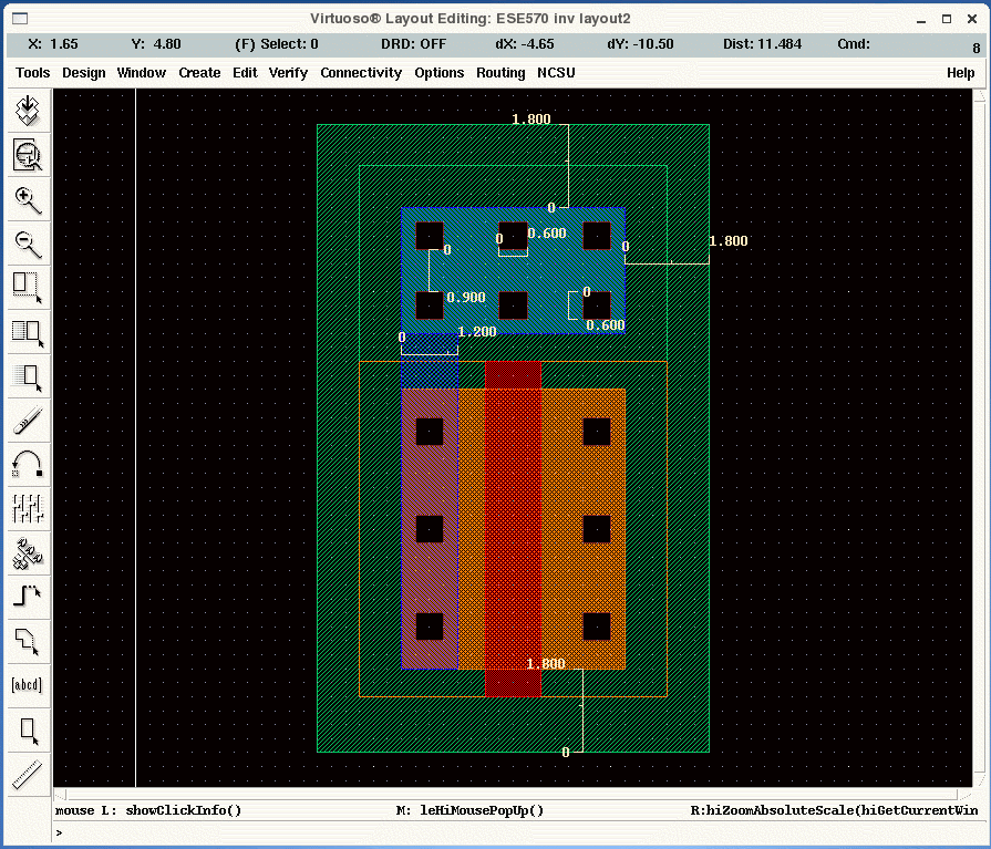
Next we need to connect the active regions to metal lines so that they can be routed. The figure below shows the metal1 layer (blue line-shaded polygons) is connected to the active region by an active contact (cc.dg, which is solid black). Remember that the design rule usually restricts the size of the contact to be 2lambda * 2lambda, which is 0.6u * 0.6u. The nselect creates an n+ diffusion in the nwell. This is the body pin of the pmos transistor, which should be connected to power (vdd!). We'll touch on how to connect to the power supply later.
Also, a point of thought usually is how much distance there should be between all these strange looking polygons. That is governed by the design rules, the link for which is given at the website MOSIS Layout Design Rules. You should at least be familiar with some of these rules (e.g. contact size should always be 2 lambda * 2 lambda, distance between poly and active region, etc.). Once you get into the habit of designing manual layouts, you will start to remember the more common design rules. For now, you will have to perform a Design Rule Check (DRC) every now and then on your layout in order to make sure that you have satisfied the rules. More on this can be found on the next page of this online Cadence tutorial.
-
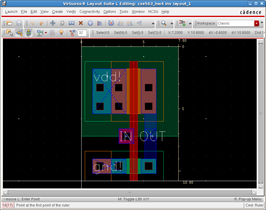
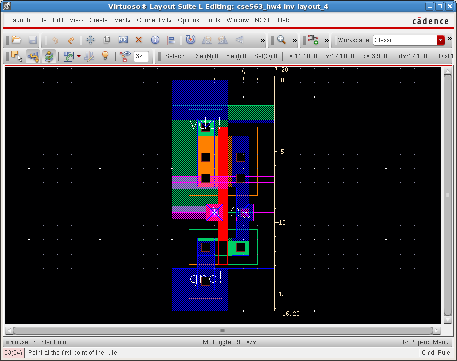
Next, you can proceed to create the nmos transistor but this time your nmos needs to be created in the nselect layer while the p+ diffusion of the NMOS is in the pselect. The size of the nmos chosen in this design has the same length as the pmos (1.2um) but the width of the nmos is chosen as 3um instead. Note that since we are using an nwell technology, we don't need an explicit well for the nmos transistor (the pwell) since the background is p-substrate. The figure below shows the inverter.
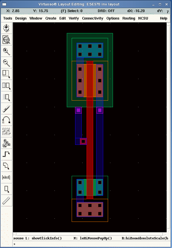
We have chosen to space the nmos and the pmos by the distance of 15um active-to-active distance for a 0.6um process. This region between the two transistors would be used for pin definitions and for routing signals from one layout cell to another. The more the distance between the nmos and the pmos transistor, the more connections can be routed and less problems to worry about in the future when designing big cells. However, a large distance may be inefficient and result in a very big layout. But for the sake of learning, we would rather choose to go with a large distance of around 15um. Note that you can stretch the distance between the active layers to make the cell shorter. One way would be to use the s command on the poly and metal1 vertical strip layers to stretch the layers upwards. You can then move the rest of the nmos transistor up by highlighting the bottom portion of the layout with your mouse (all of the edges will be highlighted in white) and using the m (move) command. Once you are in the move mode, just click once on the highlighted portion of the layout and move it upwards. Click again to release the selected layers. A good way to know if you are in the move mode is to look at the lower left-hand corner of the inverter layout view and read the messages there. You should see the following: Select the figure to be moved:
The gate of the transistors needs to be connected to the metal1 lines for it to be accessed. To do that you will be using a contact "cc.dg" to make a contact between an already overlapping metal1 and poly layer. Similarly, we desire to then connect the metal1 to metal2 (though it is not necessary) for pin connections. For this purpose, we will make a contact between a metal1 and a metal2 using a "via". There are two ways of doing this.
Method 1: Bring metal1 and metal2 to overlap each other and then draw a "via.dg" rectangle of 2lambda * 2lambda (which is 0.6u*0.6u for AMI 0.6u process). Similarly, bring poly and metal1 together and then draw a "cc.dg" rectangle of 2lambda * 2lambda.
Method 2: There are some ready-to-use macros available for making contacts. To access a macro cell which has a poly-metal1 combo with a single contact, instantiate the cell " M1_P" (note capital letters) from the library "NCSU_TechLib_ami06". Similarly, to access a metal1-metal2 combo with a via, instantiate the cell "M1_M2" from the NCSU_TechLib_ami06 library. These cells will appear as a black box. To see through the cell, type "Shift -f". This will make the cell visible. Remember that you cannot update this cell, since it is a standard library cell.
The figure below shows the connection. The red-shaded polygon with a black square at the center and blue borderline is the M1_P contact. The blue-shaded polygon with a pink square at the center and pink borderline is the M1_M2 contact.
-
For simulation purposes and standard cell design rules, it is necessary to add the pin (pn) layer. They are identical in purpose to the input/output and vdd!/gnd! pins in the schematic view. Power and ground rail pins should be declared as jumpers. Input/output pins should be in metal2 while power/ground rail pins should be in metal1. It would not be a bad idea to label your pins with the text layer, but make sure to name the labels the same as the pins in your schematic and put them on top of the labeled wires. Click on metal2.pn in the LSW window. Then press Ctrl-p in the layout editor window. A window will pop up. Enter the name "inp" for labeling input. Choose "Display pin name" option and define the pin as input. Then click on the left mouse button with the cursor placed at the top left corner of the metal2 square to be labeled. Then drag the mouse to the right bottom corner of the same metal2 square to be labeled. Click one more time inside the metal2 square to place the text. Do the same steps for placing an "out" pin except for the fact that you declare the pin as "output".
-
Next we want to label the vdd! and gnd! pins. To do this, select the metal1 pn pattern, which is just a blue rectangle outline with an X across. To draw the labels, type Ctrl-P. A pop up menu will appear. Type vdd! for the Terminal Names field and select the I/O type as jumper. Then move your cursor to the starting point of the label and click on the left mouse button. Move your cursor to size the label and click on the left mouse button again. Likewise, label the gnd! pin. The figure below shows the pin labels for vdd! and gnd!
Note that at any time, you can view the properties of any layout element you placed in your layout view by highlighting the particular element with the mouse and using the p (properties) command. This is especially helpful when you want to identify a particular via or pin that you have just created.
There are many other useful layout commands and features available through Cadence and most of these options have their own hotkeys. A very good idea would be to take a little bit of time to go through the many layout functions in the menus located at the top of the layout view (eg. Window, Create, Edit, Connectivity, Options) and maybe even try some of them out on your initial layout design. You can always undo your last performed function by clicking on Edit → Undo or by pressing the u button.
| Operation | Description |
|---|---|
| Move about the layout view screen | Keyboard arrows (up, down, left, right) |
| Fit entire layout onto screen | f |
| Zoom in/out | Ctrl/Shift z |
| Save design | F2 |
| Cancel previous command | Esc |
| Reveal all mask layers within each layout cell | Shift f (Use Ctrl f to hide these layers) |
| Properties | q |
| Create path | p (Convenient for making interconnections between I/O pins of layout cell; need to select mask layer first from LSW window) |
| Create rectangle of mask layer | r (Select .dg mask layer first from LSW) |
| Create pin | Ctrl p (Select .pn mask layer first from LSW) |
| Instantiate layout cell | i |
| Select more than one mask layer simultaneously | Hold down Shift and click on each layer (Use Ctrl to deselect a particular layer) |
| Undo | u |
| Copy | c |
| Delete | d |
| Move | m |
| Stretch | s (Point to edge of mask layer first using mouse cursor) |
| Ruler | k (Erase ruler – Shift k) |
CONGRATULATIONS!!! You've just created your first inverter.
When working with routing different cells and in the design of bigger cells, please make sure that you pay attention to the following issues:
- Avoid using polysilicon (poly) as a long wire. Use it only for local, < 6 um, connections since its sheet resistance is quite high (15-30 Ohms/square), as well as its capacitance over field oxide.
- Use thick wires for power rails, minimum 4 lambda, especially if they are long and supplying a lot of current. Keep in mind that the typical current density rating for metals is 0.5 mA/micron. Size them appropriately for the value of the current they carry.
- When changing metal layers, the number of contacts to use should follow from the current rating of the contacts themselves. The current density for each contact should be kept below 0.5 mA/micron.
Design Rule Check (DRC)
Our next step in the Design Process is to perform a Design Rule Check, more commonly known as DRC, on the layout. Although designers might be conscious of the design rules when performing the layout, there is a possibility of overlooking and thus violating the design rules. So, the DRC is a step taken to prompt us of any violations. This step is important because the violation of any design rules would result in a higher probability, and in some cases an absolute certainty, that the fabricated chip does not work as desired.
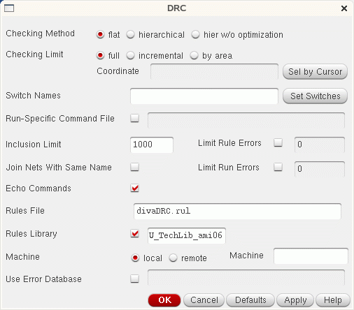
To run the DRC, choose DRC... from the Verify menu in the layout view window. A pop-up menu will appear.
You need to make sure that you're in edit mode for your layout that you want to run DRC on. For huge layouts, DRC might take a bit of time to perform. You can shorten this time by deselecting the Echo Commands option. Click on the OK button.
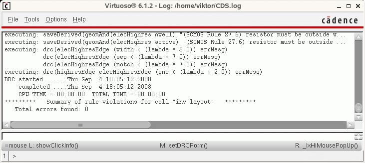
Cadence then runs the DRC and reports the errors or warnings, if any, in the CIW window.
The CIW window above shows that there are no errors or warnings found in the DRC process.
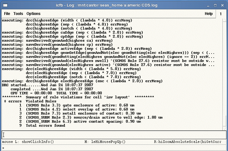
Let's perform a DRC on a layout that has errors. For the purposes of this tutorial, this step is strongly recommended so that you can gain some experience in dealing with layout DRC violations. You can purposely violate a design rule by stretching any of the mask layers to some ridiculously large dimension or by moving/shifting some layer as shown below. In this case, the pactive and cc.dg contact layers are shifted slightly to the right.
The layout above leads to the results of the DRC. Errors are indicated by markers (white as shown above) but in your layout, these markers will blink. The errors are also reported in the CIW as shown below.
- You may then proceed to correct the errors according to the design rules. Taking the above as an example, SCMOS Rule 6.2 states that the minimum spacing between active and contact layers is 0.90 um.
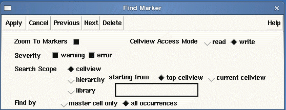
When performing huge layouts, the blinking markers might not be easily located at times. Fortunately, Cadence has an easy search tool. Under the Verify menu in the layout window, choose Markers → Find...
A pop-up menu will appear. Click on the Zoom to Markers box.
Click on the Apply button and Cadence will zoom in to the errors or warnings as desired. If there are more than one errors/warnings, as is almost always the case, you can view each one of them by clicking on Next.
Layout: Extracting Parasitics
A successful DRC ensures that the layout passes through the rules designed for faultless fabrication. However, it does not guarantee if it really represents the circuit you desire to fabricate. In our case, for an inverter, we really need a tool than can compare the connectivities of our layout with that of the schematic and ensure that it is really a layout for an inverter. One way Cadence does this is by generating an Hspice netlist file from the layout and comparing it with the netlist for the schematic. This is the essence of the LVS tool. Before performing an LVS, the layout has to be extracted.
-
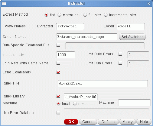
The first step is to extract all the connectivities and parasitic capacitances from your layout design. From the layout view window, choose Extract... under the Verify menu. A window will pop-up. Make sure that the entries are as given below. For the entry in Switch Names, click on Set Switches. A window will pop-up. Choose the option for Extract_parasitic_caps. Note that, if for some reason, you did not want to extract the parasitic capacitances, you would leave the Switch Names empty. Finally, click on OK. The beauty of this extraction tool is that Cadence will recognize not only all the connections but also more importantly, if you have designed the layout correctly, it will also recognize all the nmos and pmos transistors.
Make sure that your layout window is in Edit mode.
-
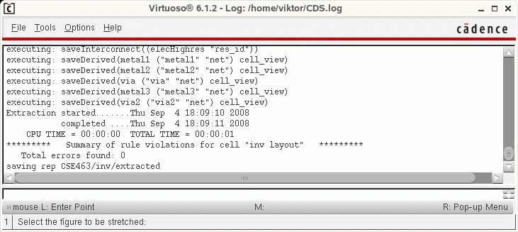
Your layout will then be extracted and while Cadence is doing so, the intermediary steps will be displayed in the CIW. It will tell you whether the extraction is successful or not.
Layout: Layout vs. Schematic (LVS)
The next step is to perform LVS. Since we generated a layout with certain a W and L for the transistors (for the case discussed here, the author had nmos W = 3u and L = 1.2u and pmos with W = 6u and L = 1.2u), the layout versus schematic operation (discussed below) will give you an error if the schematic against which the layout is compared has a different W and L for its pmos and nmos transistors. So, make sure that the nmos and pmos have correct entries in their properties field for W and L.
Before you are about to perform LVS, you need to make sure that Cadence is checking for certain LVS rules. To do so, click on NCSU → Modify LVS Rules … from the layout view window of your inverter. A window should pop-up with a number of LVS options available for you to choose. For our purposes, you should verify that the following 4 items are selected:
Allow FET Series Permutations, Combine Parallel FETs, Combine Parallel Capacitors, Compare FET Parameters
This check should be performed every time you are about to start an LVS.
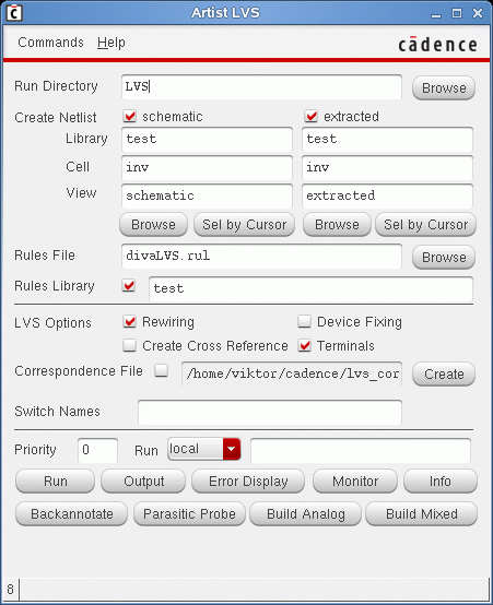
From the extracted window, choose LVS... under the Verify menu. A pop-up menu will appear. Type in the Run Directory that you want to run the LVS in, as well as the cell names that you want to run LVS on and all the other fields as shown in the inverter example below. It is advisable to put the run directory in the /tmp/username as you might run out of disk quota when designing huge layouts. If you already had an LVS directory, a window will pop-up which might say "The selected LVS rule directory does not match the run form". Just select Form Contents and click OK.
Click on the Run button and wait.
A pop-up menu will then appear notifying you of the successful completion or failure of the LVS job. If successfully completed the job, you will see the following dialog box.
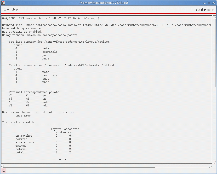
Click on the OK button. Click on the Output button in the Artist LVS window. You should see the following message:
We see from the dialog box that there are no errors in the LVS comparison. However, there could have been errors if, for example, the W and L values of the transistors in the schematic window did not match with the W and L values of the transistors in the layout. If there are any errors, click on Error Display in the LVS menu to view what went wrong. It is very beneficial if you click on Help in the si.log output window shown above. It will explain each of the terms in the above window in great detail. The si.log will also explain to you all the errors that it detected in both the schematic and layout views during the LVS comparison.
The following points illustrate a situation if we had an error in the previous step.
- By clicking on Error Display in the LVS window, the LVS Error Display window will pop-up. Select or deselect the various options so that the errors that will be shown are only those that you want to see at this point. In our case, the only errors we encounter is the size errors and to see that, we select parameters under the Unmatched field.
- To zoom into each error, select the Auto-Zoom option and then click on the First button from the Display buttons. To view each error in sequence, keep clicking on the Next button. You will see each error being highlighted by whatever color you selected from the Error Color menu in the extracted window. The default color should be "hilite.d1". You should pick a color that is easy for you to see in the extracted view.
- To get more information about the error, click on the Explain button. Then move your cursor above the highlighted point/area and click on the left mouse button. A pop-up menu will appear. Sometimes the information given is not very helpful. This is where your problem-solving skills come to play and are being sharpened.
- Modify the layout or schematic appropriately and rerun the LVS check till your layout design is perfectly matched to the schematic view.
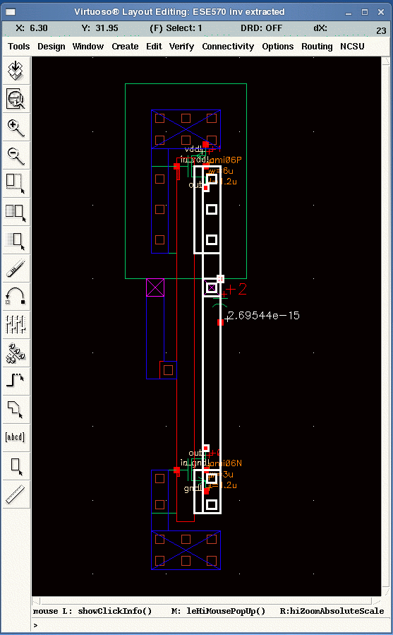
- There is also a feature that can help you in debugging the layout; especially in checking the connections of your nets. Move your cursor to the net you want to highlight and click on the left mouse button. Anything that is connected to that net will be highlighted in white. You are then able to determine which connection or connections should not have been made to that net based on what has been highlighted. An example of the highlight is shown below.
One should realize that almost no one designs a perfect layout on the first attempt so do not expect to pass the LVS check on your first try. In most cases, there will be many errors reported by both the si.log file and the Error Display window. You should not be intimidated by all these errors. Many of these are, in fact, related to each other. Hence, once you fix one of these errors, many of the other errors should disappear. The idea is to concentrate on one error at a time, change the layout design accordingly and repeat the extraction and LVS steps until the layout and schematic views match perfectly with each other.
Post Layout Simulation
The parasitic capacitances extracted according to how your layout is designed might be critical in affecting the actual performance of your design. In order to get an idea of how the design would work from your layout, you should perform a post-layout simulation from the extracted view. The procedure is identical to that for simulating from the schematic view.
Our main goal here is to obtain the netlist of the layout design from Cadence in the Spectre format so that we can run a Spectre simulation from the LINUX prompt. This method is preferable for CSE463 students and people who like to write and edit the Spectre code themselves. However, for all others you may as well want to use the complete Affirma Analog Environment simulation tools to perform your simulations.
Open up the test schematic for the inverter in edit mode. You will see the following window:
Under the Launch menu, choose ADE L. A window similar to the one shown below will pop-up.
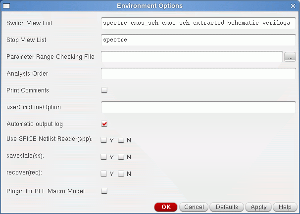
Click on Setup → Environment… and you will see the Environment Options window open up. Originally, the Switch View List should contain the following items:
spectre cmos_sch cmos.sch schematic veriloga ahdl
In order for Cadence to simulate through the extracted view of the layout design instead of the schematic view, you will include an additional item (extracted) in the Switch View List such that it now contains the following:
spectre cmos_sch cmos.sch extracted schematic veriloga ahdl
The Enviroment Options window should look like the one bellow:
Press OK. You can now perform the simulation in the same manner as before using ADL Spectre methods. This additional step allows you to take into account all the parasitic capacitances (eg. from interconnects and source/drain areas) that were extracted into the extraction view from your layout design. You may be able to notice subtle differences in the post-layout simulation results or waveforms as compared to the pre-layout schematic view results.
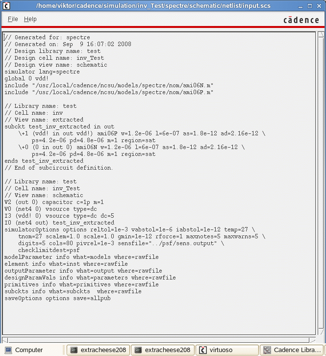
To be absolutely sure that Cadence is running simulations through the extracted view, you can view the generated a netlist by clicking on Simulation → Netlist → Create … from the Analog Environment Simulation window. The generated netlist will open up in another window. Within the first 20 or so lines, you should be able to search for a single line of code that confirms that the extracted view was indeed taken. This line of code should look something like the following:
// Library name: test
// Cell name: inv
// View name: extracted
The last line points to the file which will be used for simulation. In this case the extracted view of cell name inverter will be used.
Verilog Hardware Description Language
Verilog is a description language that describes the behavior of a logic circuit at gate level. It can also be used for simulation of a logic design. It does not just simulate the function of the circuit but also the delays for switching each gate.
The first step in running a Verilog simulation is to create the behavioral or functional model files for the circuit that you wish to simulate. From the schematic file you can then run the simulation of the total design you have created. The last step is to evaluate the results from the input and output waveforms.
This section will enable you to create a Verilog file for your design (an example considered here is that of an inverter). You will also simulate this inverter using Cadence.
Creating a Verilog Model for an Inverter
We'll now create a Verilog description of the inverter.
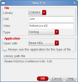
In your library manager click once on the CSE463 library and then click once on the inv cell view. Now left click Library manager: File → New → Cell view. In the dialog box type behavioral in the View field. Select Verilog for the Type. The New File window should look like the one below:
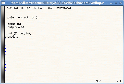
Left click OK. The text tool should now appear, with some basic template stuff inside. Anything preceded by a "//" is considered to be a comment.
An Emacs editor window will pop up. Add the following the statement in between the module statements:
not (out, in);
If the input and output names are not "in" and "out" for you, substitute them with your own names. The (out, in) syntax specifies the output and input for the inverter. In Verilog, the convention is that the output arguments of the module (gate) are listed before going on to the inputs.
This is all the text you need in order to describe your inverter. Now you can save the text file and close it. Cadence will tell you in the CIW whether the functional view is successfully parsed (no syntax errors) or not.
Now you are ready to simulate your Verilog code.
The commands that you used in the text file are described below:
- module
- Defines the beginning of a Verilog module.
- inv(...)
- Specifies the name of the module. All pins (connections to the outside world) must be specified inside the parenthesis.
- in/out
- Defines what the input/output pins into the module are.
- not
- Tells that this gate is an inverter. There are three basic gates: AND, OR, NOT, NAND, and NOR.
- endmodule
- Signifies the end of this particular module.
The final model file should look like the one below:
Verilog Simulation
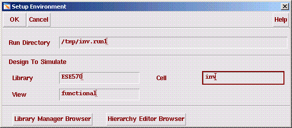
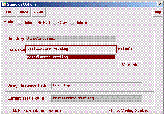
Left click CIW:Tools → Verilog Integration → Verilog-XL. The Setup Environment windows should appear. Fill in the appropriate fields as shown in the figure. It is recommended that you run your simulation in the local /tmp directory on the machine. Usually your simulation will run faster.
Left Click OK.
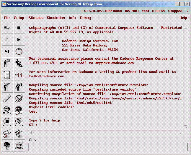
A pop up window will appear. This window is called the Verilog-XL Integration Control window. Start the simulation process by first clicking on Setup → Record Signals in the Verilog-XL Integration window. Make sure to choose All Signals as shown below.
Left Click OK.
There are (for us) three very important buttons on the control panel. The two that are currently active (not grayed out) are Start Interactive in the upper left corner of the panel, and the View Waveforms button in the lower right corner of the panel. The third is the Continue button (currently grayed out) in the second row, second button of the panel. Next, click on the Start Interactive (top-left) button in the list of buttons provided in the Verilog-XL Integration Control Window or select Simulation → Start Interactive.
Click on the Stimulus → Verilog menu item. You will get the Stimulus Options window as shown below. Select the Edit button and press OK. This will help you create a stimulus file for the simulation of an inverter.
An Emacs window will appear. Modify the file as shown below:
The above stimulus file starts with the input inp = 0 and then changes to 1 at the time instant 25. Then it changes to 0 at 35 time instants later (25+35=60 time instants) and then to 1 at 75 instants (25+35+75=135 time instants) later. The simulation time is 235 units. The exact time of simulation is governed by the timescale command in the original functional view file.
Click on the Continue icon (second top icon in the second column) in the Verilog-XL Integration Control window or select Simulation → Continue. The Verilog simulation will begin. Pay attention to the messages that appear in the Verilog-XL Integration Control window to verify that the simulation is indeed running. You will be notified by those messages in the window when the simulation has finished.
Next click on the very bottom right icon (View Waveforms icon) or select Debug → Utilities → View Waveform. A pop up window will appear. It is the window in which you will view your simulation results and is called SimVision.
From top right part of the SimVision window, select Send to Browser icon (the icon with a magnifying glass). The following window should open.
Now select the waveforms that you want to plot. After you selected the waveforms, press the Send to Waveform button (It is located right next to the Send to Browser button.
The waveforms should be as follows:
Note: To see the complete waveform, please select View → Zoom → Out or the equality button right above the waveform window.
Example Layouts
Inverter
Here are several different ways to layout an inverter:
This inverter layout is designed to abut to form a ring oscillator. Notice the Metal 2 trace above the IN/OUT terminals. This provides the return path from the output of the last inverter to the input of the first inverter in the ring oscillator. Also, the bulk contacts are located above and below the PMOS and NMOS transistors so as to save horizontal space.
Ring Oscillator
Shown below is an 11-inverter ring oscillator:
2-Input NAND Gate
2-Input NOR Gate
Complex Function 1
Z = (AB+C)D
Z = ((A' + B')C' + D')'
Complex Function 2
Y = (A B'+C)G'+E F'
Y = (((A'+B)C'+G)(E'+F))'
2x1 Multiplexer
Advanced Topics
Pad frame
One tiny chip unit is 1.5mm x 1.5mm. The pad frame provided here has a total of 40 pins. The 4 corner pins are used for VDD and GND (note the +/- symbols in the layout) and the remaining 36 pins are available for I/O.
To use the pad frame, please do the following steps:
- Download Padframe_C5N.tgz into $HOME/cadence/library.
- Type "cd $HOME/cadence/library".
- Type "tar -xzvf Padframe_C5N.tgz". This will extract the pad library.
- Type "cd ..".
-
Edit cds.lib and add the following line:
DEFINE pad library/pad
- Execute virtuoso. The pad library will now appear in the Library Manager.
The pad frame layout is shown below.
Vector File Simulation
Now we are introducing a new simulation method under Cadence Spectre Simulator: Using Vector File. Vector file is a very convenient way to do large scale digital simulation, the manual for how to write digital vector file can be download from here:
In Cadence, first we create a NAND2 cell schematic view:
In this NAND2, we have two input ports: A and B, one output ports: C. Then in vector file, we assign values to A and B. The example vector file NAND2.vec:
In a basic vector file, you need define the radix, i/o, tunit, and value for the input or output ports, moreover, you can also define your rise/fall time, high/low voltage. Next, we open the Cadence ADE L:
Then left click Setup->stimuli..., the window of stimuli will jump out:
Then left click to select the Globe Sources at the first row, then select vdd!, click select enable, fill the DC voltage with a value, here we just define it 3V, (Note: by giving the value to vdd! here, we don't need to load vdc module anymore), then click apply:
After we click OK, the window will disappear, we left click Setup-> Simulation Files, then select "Vector Files" tab at the top row, add NAND.vec as the Vector Files:
Click OK, then left click choose Analyses-> Choose..., on the "Choosing Analyses" tab, select tran, then fill the stop time with a value, here we fill it as 40n s:
Click OK, then select the ports you want to view in the schematic by using Outputs-> To Be Plotted-> Select On Schematic, then click Netlist and Run button:
Finally, we get the waveform of this NAND2 gate:
Acknowledgement
This tutorial was originally created by Viktor Gruev. Michael Hall has updated and is currently maintaining the tutorial.
Information is provided "as is" without warranty or guarantee of any kind. No statement is made and no attempt has been made to examine the information, either with respect to operability, origin, authorship, or otherwise.
Please use this information at your own risk--and any attempt to use this information is at your own risk--we recommend using it on a copy of your data to be sure you understand what it does and under what conditions. Keep your master intact until you are personally satisfied with the use of this information within your environment."
Cadence® is a trademark of Cadence Design Systems, Inc., 555 River Oaks Parkway, San Jose, CA 95134
For web related questions contact: Viktor Gruev, Michael Hall

