Difference between revisions of "Tutorials:Cadence:ExampleLayouts"
m |
|||
| (7 intermediate revisions by the same user not shown) | |||
| Line 3: | Line 3: | ||
== Inverter == | == Inverter == | ||
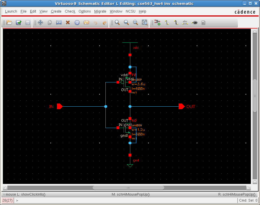
| − | + | Here are several different ways to layout an inverter: | |
| + | |||
| + | ;Schematic | ||
| + | :[[File:Tutorials-Cadence-ExLayout-Inv-Sch.png]] | ||
| + | |||
;Layout 1 | ;Layout 1 | ||
| Line 24: | Line 28: | ||
:Area = 7.20um x 16.20um = 116.64um<sup>2</sup> | :Area = 7.20um x 16.20um = 116.64um<sup>2</sup> | ||
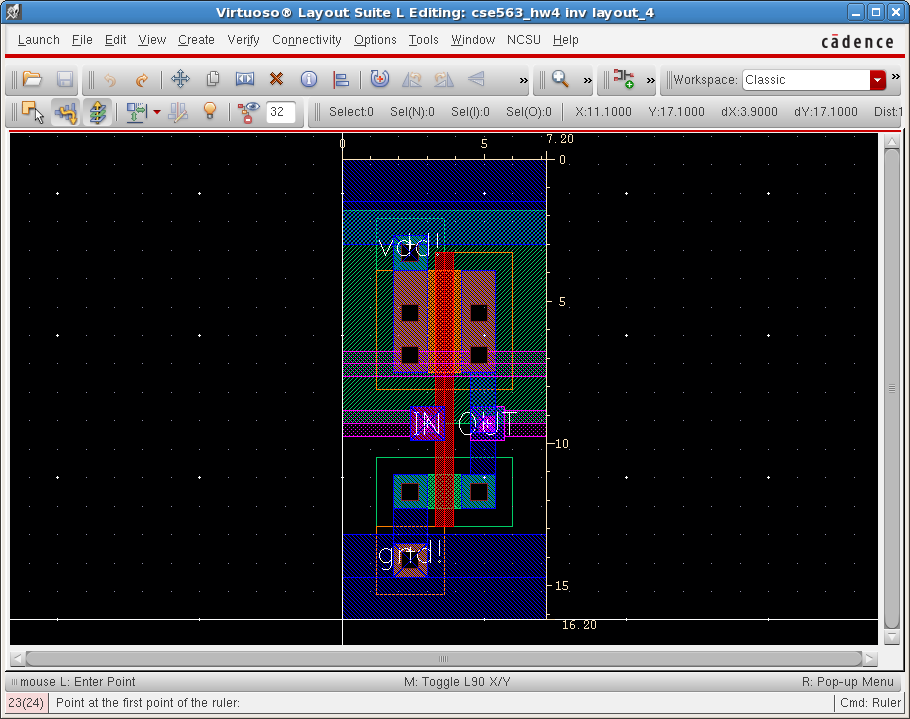
| − | This inverter layout is designed to abut to form a ring oscillator. Notice the Metal 2 trace above the IN/OUT. This provides the return path from the output of the last inverter to the input of the first inverter in the ring oscillator. | + | This inverter layout is designed to abut to form a ring oscillator. Notice the Metal 2 trace above the IN/OUT terminals. This provides the return path from the output of the last inverter to the input of the first inverter in the ring oscillator. Also, the bulk contacts are located above and below the PMOS and NMOS transistors so as to save horizontal space. |
| + | |||
| + | |||
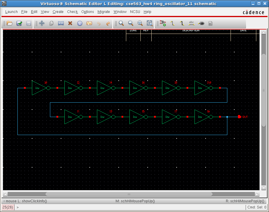
| + | == Ring Oscillator == | ||
| + | |||
| + | Shown below is an 11-inverter ring oscillator: | ||
| + | |||
| + | ;Schematic | ||
| + | :[[File:Tutorials-Cadence-ExLayout-RO-001.png]] | ||
| + | |||
| + | |||
| + | ;Layout | ||
| + | :[[File:Tutorials-Cadence-ExLayout-RO-002.png]] | ||
| + | :Area = 55.20um x 16.20um = 894.24um<sup>2</sup> | ||
| + | |||
| + | |||
| + | == 2-Input NAND Gate == | ||
| + | |||
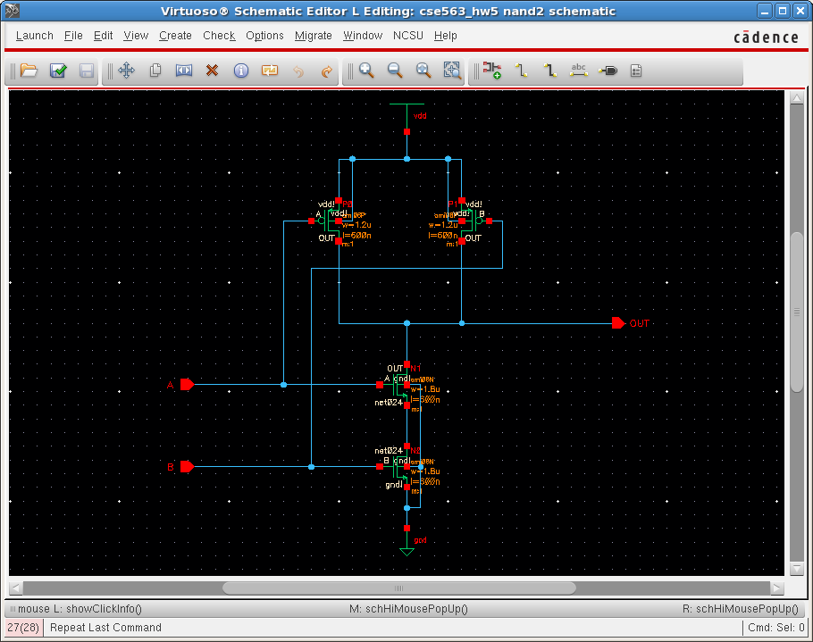
| + | ;Schematic | ||
| + | :[[File:Tutorials-Cadence-ExLayout-nand2-Sch.png]] | ||
| + | |||
| + | |||
| + | ;Layout | ||
| + | :[[File:Tutorials-Cadence-ExLayout-nand2-001.png]] | ||
| + | :Area = 9.60um x 15.60um = 149.76um<sup>2</sup> | ||
| + | |||
| + | |||
| + | == 2-Input NOR Gate == | ||
| + | |||
| + | ;Schematic | ||
| + | :[[File:Tutorials-Cadence-ExLayout-nor2-Sch.png]] | ||
| + | |||
| + | |||
| + | ;Layout | ||
| + | :[[File:Tutorials-Cadence-ExLayout-nor2-001.png]] | ||
| + | :Area = 8.70um x 17.10um = 148.77um<sup>2</sup> | ||
| + | |||
| + | |||
| + | == Complex Function 1 == | ||
| + | |||
| + | Z = (AB+C)D | ||
| + | |||
| + | Z = ((A' + B')C' + D')' | ||
| + | |||
| + | ;Schematic | ||
| + | :[[File:Tutorials-Cadence-ExLayout-ComplexFunc1-Sch.png]] | ||
| + | |||
| + | |||
| + | ;Layout | ||
| + | :[[File:Tutorials-Cadence-ExLayout-ComplexFunc1-001.png]] | ||
| + | :Area = 14.40um x 18.60um = 267.84um<sup>2</sup> | ||
| + | |||
| + | |||
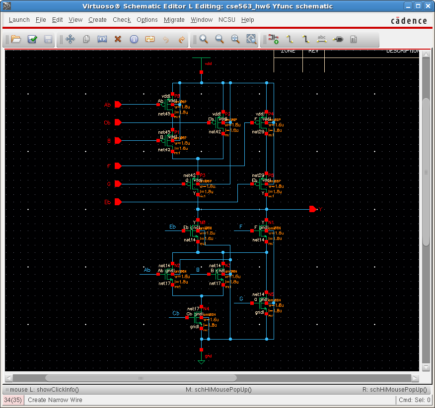
| + | == Complex Function 2 == | ||
| + | |||
| + | Y = (A B'+C)G'+E F' | ||
| + | |||
| + | Y = (((A'+B)C'+G)(E'+F))' | ||
| + | |||
| + | ;Schematic | ||
| + | :[[File:Tutorials-Cadence-ExLayout-ComplexFunc2-Sch.png]] | ||
| + | |||
| + | |||
| + | ;Layout | ||
| + | :[[File:Tutorials-Cadence-ExLayout-ComplexFunc2-001.png]] | ||
| + | :Area = 19.50um x 11.25um = 219.38um<sup>2</sup> | ||
| + | |||
| + | |||
| + | == 2x1 Multiplexer == | ||
| + | |||
| + | ;Schematic | ||
| + | :[[File:Tutorials-Cadence-ExLayout-2x1MUX-Sch.png]] | ||
| + | ;Layout | ||
| + | :[[File:Tutorials-Cadence-ExLayout-2x1MUX-001.png]] | ||
| + | :Area = 14.40um x 13.80um = 198.72um<sup>2</sup> | ||
<noinclude> | <noinclude> | ||
Latest revision as of 18:32, 16 November 2010
Contents
Example Layouts
Inverter
Here are several different ways to layout an inverter:
- Schematic

- Layout 1
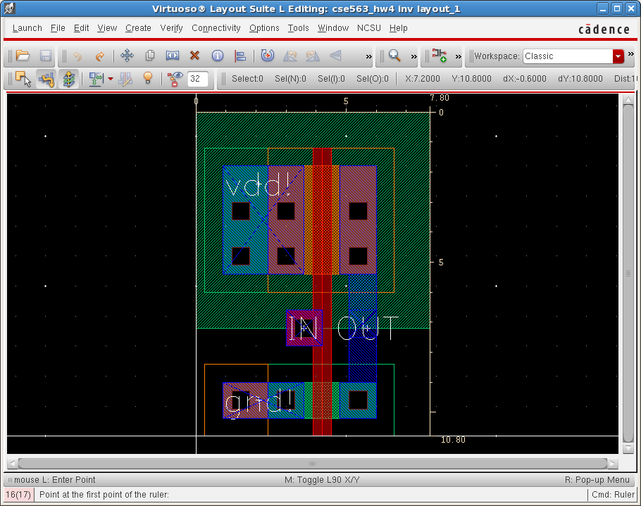
- Area = 7.80um x 10.80um = 84.24um2

- Layout 2
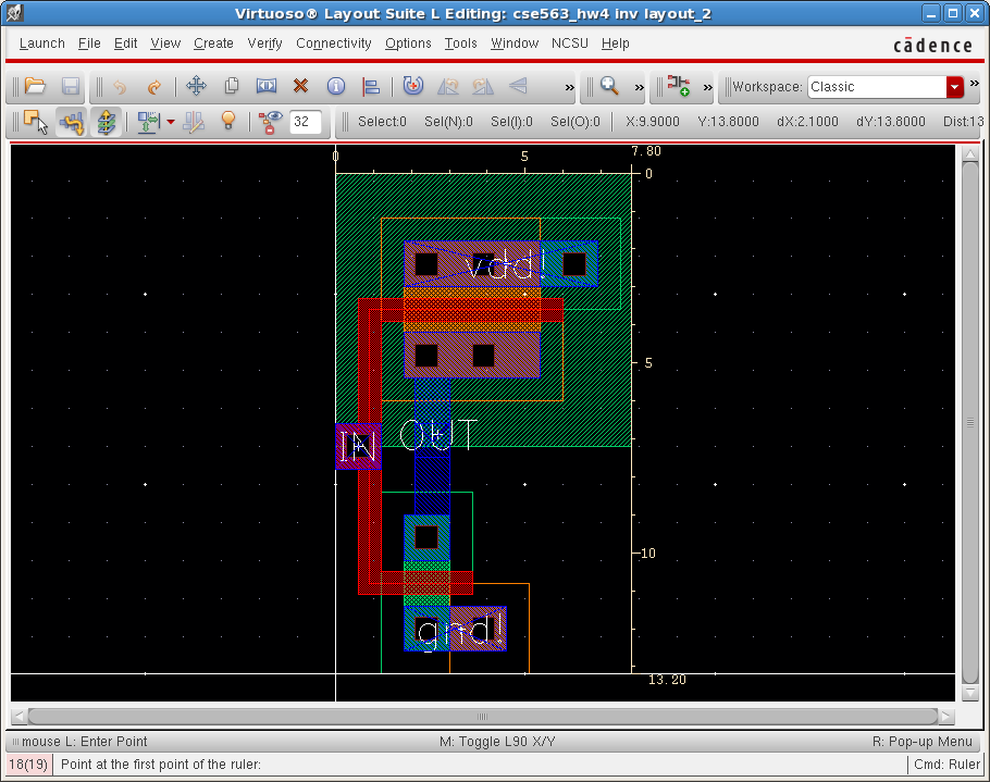
- Area = 7.80um x 13.20um = 102.96um2

- Layout 3
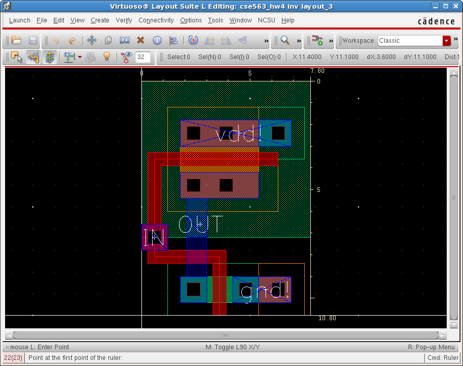
- Area = 7.80um x 10.80um = 84.24um2

- Layout 4
- Area = 7.20um x 16.20um = 116.64um2

This inverter layout is designed to abut to form a ring oscillator. Notice the Metal 2 trace above the IN/OUT terminals. This provides the return path from the output of the last inverter to the input of the first inverter in the ring oscillator. Also, the bulk contacts are located above and below the PMOS and NMOS transistors so as to save horizontal space.
Ring Oscillator
Shown below is an 11-inverter ring oscillator:
- Schematic

- Layout
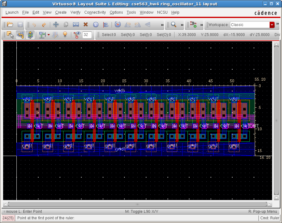
- Area = 55.20um x 16.20um = 894.24um2

2-Input NAND Gate
- Schematic

- Layout
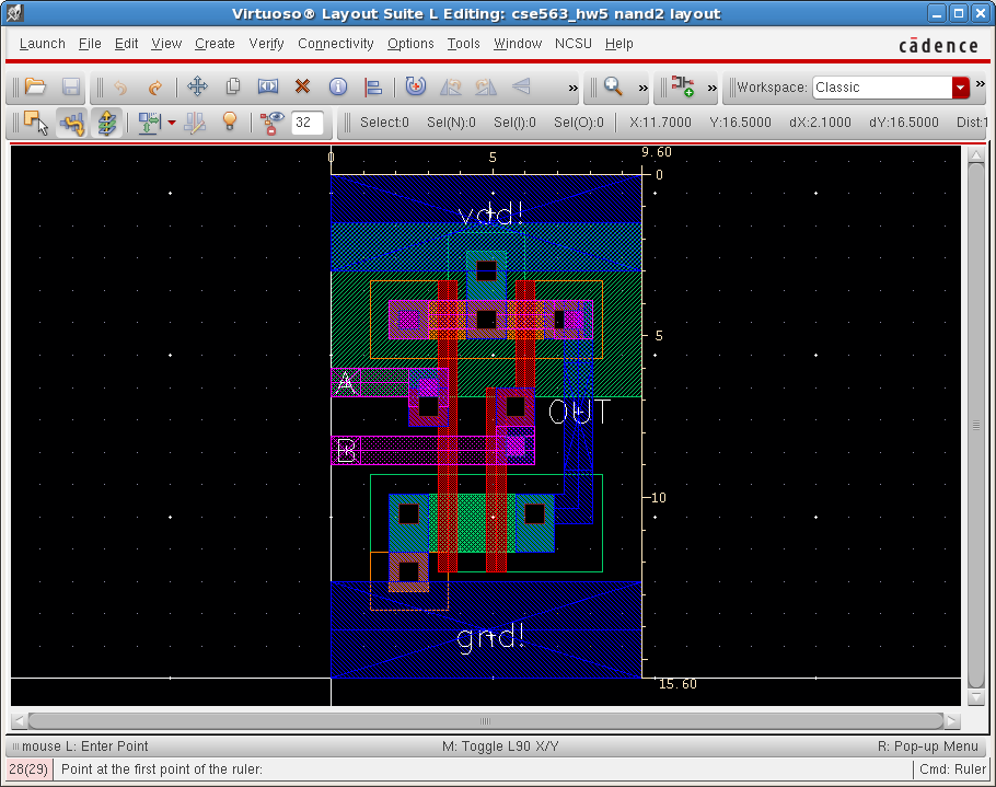
- Area = 9.60um x 15.60um = 149.76um2

2-Input NOR Gate
- Schematic
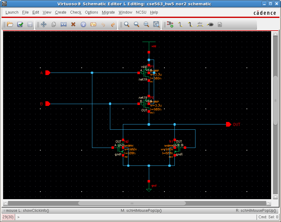

- Layout
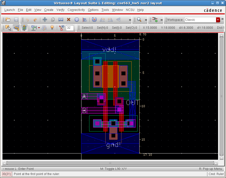
- Area = 8.70um x 17.10um = 148.77um2

Complex Function 1
Z = (AB+C)D
Z = ((A' + B')C' + D')'
- Schematic
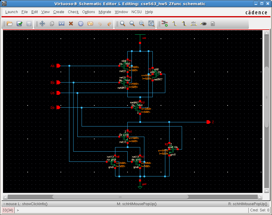

- Layout
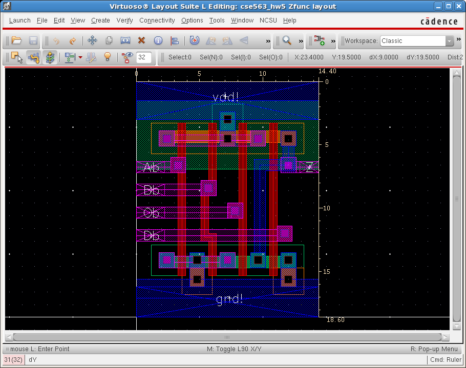
- Area = 14.40um x 18.60um = 267.84um2

Complex Function 2
Y = (A B'+C)G'+E F'
Y = (((A'+B)C'+G)(E'+F))'
- Schematic

- Layout
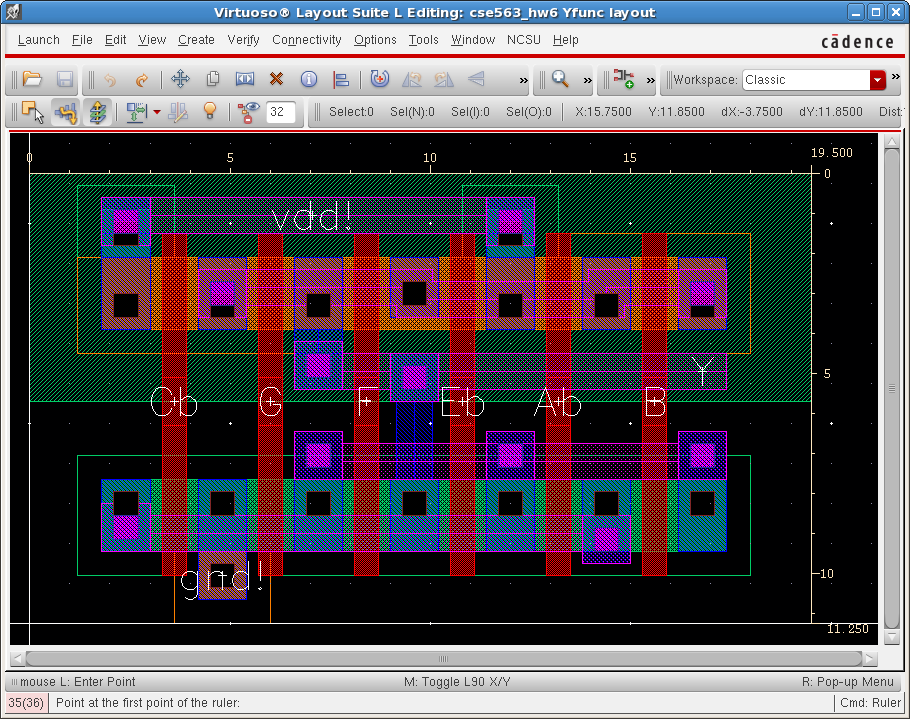
- Area = 19.50um x 11.25um = 219.38um2

2x1 Multiplexer
- Schematic


- Layout
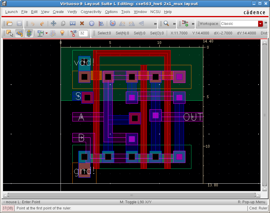
- Area = 14.40um x 13.80um = 198.72um2

Information is provided "as is" without warranty or guarantee of any kind. No statement is made and no attempt has been made to examine the information, either with respect to operability, origin, authorship, or otherwise.
Please use this information at your own risk--and any attempt to use this information is at your own risk--we recommend using it on a copy of your data to be sure you understand what it does and under what conditions. Keep your master intact until you are personally satisfied with the use of this information within your environment."
Cadence® is a trademark of Cadence Design Systems, Inc., 555 River Oaks Parkway, San Jose, CA 95134
For web related questions contact: Viktor Gruev, Michael Hall