Difference between revisions of "Tutorials:Cadence:SchematicSimulationDCAnalysis"
(Created page with "= Schematic Simulation: Creating a Test File for Simulating an Inverter = Now that we have built an inverter, we need to simulate it to show that our design is valid. First w...") |
|||
| (4 intermediate revisions by the same user not shown) | |||
| Line 1: | Line 1: | ||
= Schematic Simulation: Creating a Test File for Simulating an Inverter = | = Schematic Simulation: Creating a Test File for Simulating an Inverter = | ||
| − | Now that we have built an inverter, we need to simulate it to show that our design is valid. First we need to create a new cell in our CSE463library for testing the inverter. In the Library Manager, highlight the test library and left click on Library Manager: | + | Now that we have built an inverter, we need to simulate it to show that our design is valid. First we need to create a new cell in our CSE463library for testing the inverter. In the Library Manager, highlight the test library and left click on Library Manager:'''File → New → Cell View'''. |
In the Cell Name type inv_test and in the View Name type schematic. Left click on OK. | In the Cell Name type inv_test and in the View Name type schematic. Left click on OK. | ||
| − | + | : [[File:Tutorials-Cadence-Schematic_TestInv.gif]] | |
A new schematic editing tool will appear. You are going to instance the inverter that was previously created and connect its input pin to voltage source. The output pin will be connected to a capacitor. | A new schematic editing tool will appear. You are going to instance the inverter that was previously created and connect its input pin to voltage source. The output pin will be connected to a capacitor. | ||
| − | Left click | + | Left click '''Editing:Add->Instance'''. Click on the '''Library''' pull down menu and select the '''CSE463''' library. Select the '''inv''' cell. The Component Browser window should look like the one bellow. |
| − | + | : [[File:Tutorials-Cadence-Schematic_TestInv_ComponentBrowser.gif]] | |
| − | Place the inverter in the middle of the editing window. Note: you can press | + | Place the inverter in the middle of the editing window. Note: you can press '''F3''' key while you have selected the symbol you want to place and the ''Add Instance'' window will appear. In this window, you can edit some of the properties of the symbol if applicable. |
| − | Now we want to add voltage DC sources. Left Click | + | Now we want to add voltage DC sources. Left Click '''Editing: Add → Instance'''. In '''NCSU_Analog_Parts''' library; you will find ''vdc'' sources. Place them in the test circuit. Left Click '''Editing:Add → Instance.''' In '''NCSU_Analog_Parts''' library, under ''Voltage_Sources'' category, you will find ''vdc'' source. Place them in the test circuit. The Component Browser should look like the one below: |
| − | + | : [[File:Tutorials-Cadence-Schematic_TestInv_ComponentBrowserVDC.gif]] | |
| − | Select | + | Select ''Vdc'' and Add Instance window will appear. In the DC Voltage field enter '''5V'''. This window should appear as such: |
| − | + | : [[File:Tutorials-Cadence-Schematic_TestInv_AddInstanceVDC.gif]] | |
Place the symbol to the left of the inverter. | Place the symbol to the left of the inverter. | ||
| − | Now we want to add global ground and power lines. Left Click | + | Now we want to add global ground and power lines. Left Click '''Editing: Add → Instance'''. In '''NCSU_Analog_Parts''' library, under ''Supply_Nets'' category, you will find ''vdd'' and ''gnd'' sources. Place them in the test circuit. The Component Browser should look like the one below. |
| − | + | : [[File:Tutorials-Cadence-Schematic_TestInv_ComponentBrowserGND.gif]] | |
| − | Once you select the NCSU_Analog_Parts selection and select Supply_Nets, you will find | + | Once you select the NCSU_Analog_Parts selection and select Supply_Nets, you will find ''gnd'' and ''vdd'' symbols. The Add Instance windows for ''vdd'' and ''gnd'' should look like the ones below: |
| − | + | : [[File:Tutorials-Cadence-Schematic_TestInv_AddInstanceVDD.gif]] | |
| − | + | : [[File:Tutorials-Cadence-Schematic_TestInv_AddInstanceGND.gif]] | |
| − | Left Click | + | Left Click '''Hide''' and place the ''vdd'' and ''gnd'' symbols on the schematic. Place the ''vdd'' above the vdc symbol and ''gnd'' bellow the vdc symbol. |
| − | Next, we want to add capacitor to the output pin in order to simulate a load (other circuits) that our inverter has to charge or discharge. Left click | + | Next, we want to add capacitor to the output pin in order to simulate a load (other circuits) that our inverter has to charge or discharge. Left click '''Editing:Add → Component'''. From the '''NCSU_Analog_Parts''' library choose a cell named '''cap''' and specify its value to be '''1 pF'''. The Add Instance window should look like the one below: |
| − | + | : [[File:Tutorials-Cadence-Schematic_TestInv_AddInstanceCAP.gif]] | |
| − | Next we will add an output pin in the schematic. Left click | + | Next we will add an output pin in the schematic. Left click '''Editing:Add → Pin'''. Name the pin '''out''' and specify it as an output pin. Place the pin next to the output of the inverter. |
| − | Connect all the elements as shown in the figure | + | Connect all the elements as shown in the figure below. To connect different elements use '''Editing:Add → Wire'''. The final schematic should like the one below: |
| − | + | : [[File:Tutorials-Cadence-Sch_test_inv2.gif]] | |
Save the schematic and you are ready to simulate the inverter. | Save the schematic and you are ready to simulate the inverter. | ||
| − | In the schematic of inv_test, left click | + | In the schematic of inv_test, left click '''Editing:Launch → ADE L'''. The spectre window should appear. |
| − | + | : [[File:Tutorials-Cadence-Spectre_DC1.gif]] | |
| − | We want to specify the type of analysis we want to perform. We are going to select a DC analysis. Left click | + | We want to specify the type of analysis we want to perform. We are going to select a DC analysis. Left click '''Analog Artist:Analyses → Choose?''' Click on the '''dc''' button for Analysis. Click '''Component Parameter '''button for sweep variable. In the '''Sweep Range,''' fill '''0 and 5V '''for the start and stop. Left click on the '''Select Component'''. Now go back to the schematic and select the voltage source you want to sweep. Click on the vdc that is connected to the input of the inverter. This will pop-up a small window, which requests the Parameter Name. Click on '''dc '''to sweep the voltage. Go back to your Analysis Choose window, which should look like the one below, and click on OK. |
| − | + | : [[File:Tutorials-Cadence-Spectre_DC2.gif]] | |
| − | Second, we want to select which output voltages to be plotted. Left click on | + | Second, we want to select which output voltages to be plotted. Left click on '''Analog Artist: Outputs → To be Plotted → Select on Schematic'''. Click on the wire between your vdc source and the ''in'' pin of your inverter. Then click on the wire between the ''out'' pin of the inverter and the ''out'' pin. Both wires should change color indicating that these voltages will be plotted. |
Note: If you want to select a current to be plotted, then click on the square of a symbol where the current is flowing through. There will be a circle around the square node indicating that a current is selected. | Note: If you want to select a current to be plotted, then click on the square of a symbol where the current is flowing through. There will be a circle around the square node indicating that a current is selected. | ||
| Line 63: | Line 63: | ||
Your Analog Environment window should appear similar to: | Your Analog Environment window should appear similar to: | ||
| − | + | : [[File:Tutorials-Cadence-Spectre_DC3.gif]] | |
Note: in order to make your simulation more readable, it is often advisable to name special nets with uniquely identifiable names, so that when the simulation results are presented, they are more easily understood. | Note: in order to make your simulation more readable, it is often advisable to name special nets with uniquely identifiable names, so that when the simulation results are presented, they are more easily understood. | ||
| − | You are ready to run the simulation. Left Click | + | You are ready to run the simulation. Left Click '''Simulation → Run''' or click on the green traffic light icon in the Analog Environment window. The result window, as the one below will appear shortly. Explore the pull down menus in this window in order to customize your results. For instance, left click '''Axes → Strip''' in order to separate the different curves. |
| − | + | : [[File:Tutorials-Cadence-Spectre_DC4.gif]] | |
| − | To plot the results left click | + | To plot the results left click '''Waveform Window: Window → hardcopy'''. Select the option to Send Plot Only to File and also don't forget to disable the header option in order not to waste paper. You might also disable Mail Log To to prevent it from mailing you about the status of printing. |
| − | Now exit the Cadence Spice. Left click on | + | Now exit the Cadence Spice. Left click on '''Analog Environment:Session → Quit'''. Remember NOT to save the current state. If you choose to save the current state, several hundreds of megabytes will be used in order to save your last simulation. |
| + | <noinclude> | ||
| + | |||
| + | [[Tutorials:Cadence:CreatingSymbolInverter|Prev]] : [[Tutorials:Cadence:SchematicSimulationTransient|Next]] : [[Tutorials:Cadence:Main|Up]] | ||
---- | ---- | ||
{{Template:CadenceDisclaimer}} | {{Template:CadenceDisclaimer}} | ||
| + | </noinclude> | ||
Latest revision as of 18:52, 10 November 2010
Schematic Simulation: Creating a Test File for Simulating an Inverter
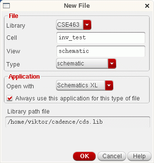
Now that we have built an inverter, we need to simulate it to show that our design is valid. First we need to create a new cell in our CSE463library for testing the inverter. In the Library Manager, highlight the test library and left click on Library Manager:File → New → Cell View.
In the Cell Name type inv_test and in the View Name type schematic. Left click on OK.
A new schematic editing tool will appear. You are going to instance the inverter that was previously created and connect its input pin to voltage source. The output pin will be connected to a capacitor.
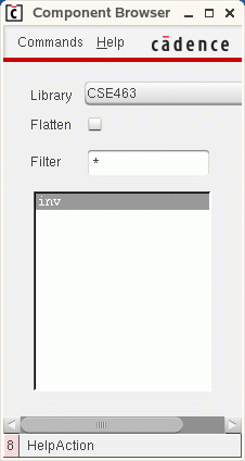
Left click Editing:Add->Instance. Click on the Library pull down menu and select the CSE463 library. Select the inv cell. The Component Browser window should look like the one bellow.
Place the inverter in the middle of the editing window. Note: you can press F3 key while you have selected the symbol you want to place and the Add Instance window will appear. In this window, you can edit some of the properties of the symbol if applicable.
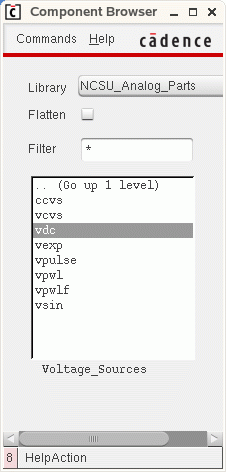
Now we want to add voltage DC sources. Left Click Editing: Add → Instance. In NCSU_Analog_Parts library; you will find vdc sources. Place them in the test circuit. Left Click Editing:Add → Instance. In NCSU_Analog_Parts library, under Voltage_Sources category, you will find vdc source. Place them in the test circuit. The Component Browser should look like the one below:
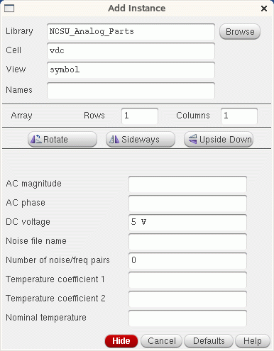
Select Vdc and Add Instance window will appear. In the DC Voltage field enter 5V. This window should appear as such:
Place the symbol to the left of the inverter.
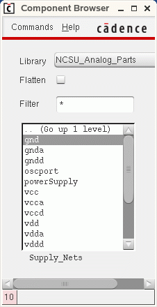
Now we want to add global ground and power lines. Left Click Editing: Add → Instance. In NCSU_Analog_Parts library, under Supply_Nets category, you will find vdd and gnd sources. Place them in the test circuit. The Component Browser should look like the one below.
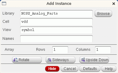
Once you select the NCSU_Analog_Parts selection and select Supply_Nets, you will find gnd and vdd symbols. The Add Instance windows for vdd and gnd should look like the ones below:
Left Click Hide and place the vdd and gnd symbols on the schematic. Place the vdd above the vdc symbol and gnd bellow the vdc symbol.
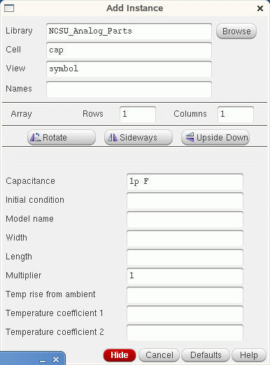
Next, we want to add capacitor to the output pin in order to simulate a load (other circuits) that our inverter has to charge or discharge. Left click Editing:Add → Component. From the NCSU_Analog_Parts library choose a cell named cap and specify its value to be 1 pF. The Add Instance window should look like the one below:
Next we will add an output pin in the schematic. Left click Editing:Add → Pin. Name the pin out and specify it as an output pin. Place the pin next to the output of the inverter.
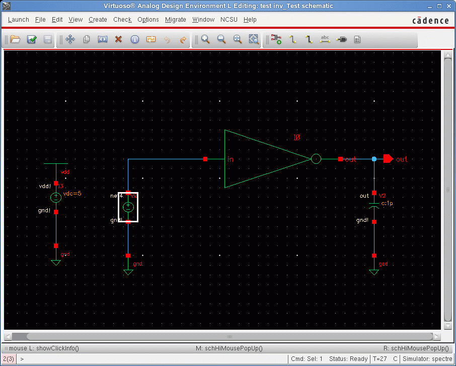
Connect all the elements as shown in the figure below. To connect different elements use Editing:Add → Wire. The final schematic should like the one below:
Save the schematic and you are ready to simulate the inverter.
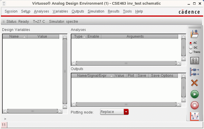
In the schematic of inv_test, left click Editing:Launch → ADE L. The spectre window should appear.
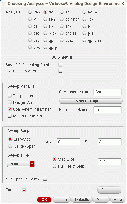
We want to specify the type of analysis we want to perform. We are going to select a DC analysis. Left click Analog Artist:Analyses → Choose? Click on the dc button for Analysis. Click Component Parameter button for sweep variable. In the Sweep Range, fill 0 and 5V for the start and stop. Left click on the Select Component. Now go back to the schematic and select the voltage source you want to sweep. Click on the vdc that is connected to the input of the inverter. This will pop-up a small window, which requests the Parameter Name. Click on dc to sweep the voltage. Go back to your Analysis Choose window, which should look like the one below, and click on OK.
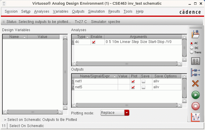
Second, we want to select which output voltages to be plotted. Left click on Analog Artist: Outputs → To be Plotted → Select on Schematic. Click on the wire between your vdc source and the in pin of your inverter. Then click on the wire between the out pin of the inverter and the out pin. Both wires should change color indicating that these voltages will be plotted.
Note: If you want to select a current to be plotted, then click on the square of a symbol where the current is flowing through. There will be a circle around the square node indicating that a current is selected.
Your Analog Environment window should appear similar to:
Note: in order to make your simulation more readable, it is often advisable to name special nets with uniquely identifiable names, so that when the simulation results are presented, they are more easily understood.
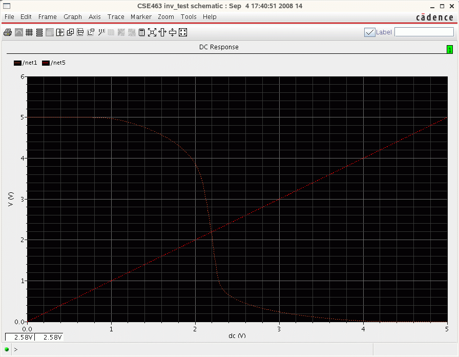
You are ready to run the simulation. Left Click Simulation → Run or click on the green traffic light icon in the Analog Environment window. The result window, as the one below will appear shortly. Explore the pull down menus in this window in order to customize your results. For instance, left click Axes → Strip in order to separate the different curves.
To plot the results left click Waveform Window: Window → hardcopy. Select the option to Send Plot Only to File and also don't forget to disable the header option in order not to waste paper. You might also disable Mail Log To to prevent it from mailing you about the status of printing.
Now exit the Cadence Spice. Left click on Analog Environment:Session → Quit. Remember NOT to save the current state. If you choose to save the current state, several hundreds of megabytes will be used in order to save your last simulation.
Information is provided "as is" without warranty or guarantee of any kind. No statement is made and no attempt has been made to examine the information, either with respect to operability, origin, authorship, or otherwise.
Please use this information at your own risk--and any attempt to use this information is at your own risk--we recommend using it on a copy of your data to be sure you understand what it does and under what conditions. Keep your master intact until you are personally satisfied with the use of this information within your environment."
Cadence® is a trademark of Cadence Design Systems, Inc., 555 River Oaks Parkway, San Jose, CA 95134
For web related questions contact: Viktor Gruev, Michael Hall
