Difference between revisions of "Tutorials:Cadence:SchematicSimulationParametric"
m (moved Tutorials:Cadence:SchematicSimualtionParametric to Tutorials:Cadence:SchematicSimulationParametric: Misspelled title) |
|||
| (One intermediate revision by the same user not shown) | |||
| Line 44: | Line 44: | ||
Both input and output waveforms are plotted on the same graph. At the top of the graph, the parameters of the different colors on the graph are explained. You can also point and select a waveform. Once selected, if you hold down the left mouse button and move the selected waveform, a text will appear describing the parameter i.e. Nmos_W value of that particular curve. You can observe that as the width of the nmos transistor is increased the Vlt value i.e. the point where Vin and Vout cross, is moved closer to ground. | Both input and output waveforms are plotted on the same graph. At the top of the graph, the parameters of the different colors on the graph are explained. You can also point and select a waveform. Once selected, if you hold down the left mouse button and move the selected waveform, a text will appear describing the parameter i.e. Nmos_W value of that particular curve. You can observe that as the width of the nmos transistor is increased the Vlt value i.e. the point where Vin and Vout cross, is moved closer to ground. | ||
| + | <noinclude> | ||
| + | |||
| + | [[Tutorials:Cadence:SchematicSimulationTransient|Prev]] : [[Tutorials:Cadence:CreatingLayoutInverter|Next]] : [[Tutorials:Cadence:Main|Up]] | ||
---- | ---- | ||
{{Template:CadenceDisclaimer}} | {{Template:CadenceDisclaimer}} | ||
| + | </noinclude> | ||
Latest revision as of 19:08, 10 November 2010
Parametric Analysis with Spectre
This tutorial will guide you through the process of performing a parametric analysis for the inverter circuit. In particular, we are going to vary the width (W) of the Nmos transistor in the inverter circuit within a specified range and see the effect on the logic threshold value (VLT)
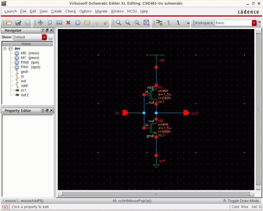
The schematic of the inverter circuit is shown below. I used nmos4 and pmos4 symbols from NCSU Analog library. You can also use your inverter that you designed earlier.
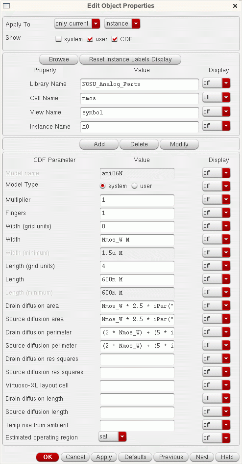
In order to be able to automatically sweep a parameters in a given circuit, this parameter must have a variable name assigned. In our example, the width of the nmos transistor is assigned Nmos_W variable name. This variable name Nmos_W is typed instead of the numeric value which we usually assign, in the nmos property box(shown below).
If other parameters are desired to be analyzed, simply assign a variable name in the appropriate box. Multiple parameters can be also simultaneously parametrically analyzed.
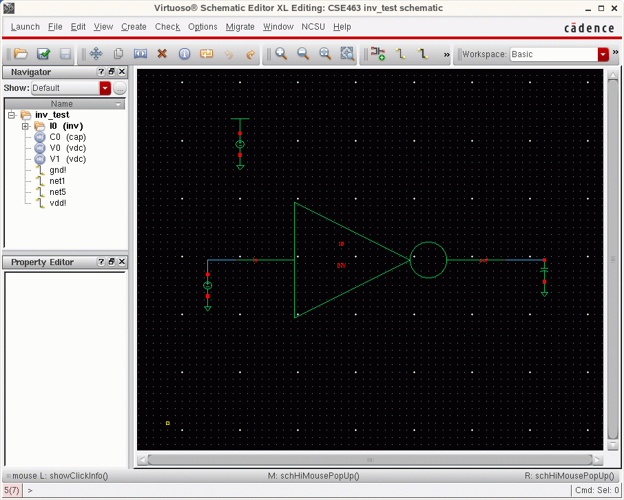
The next step is to create a test schematic for the inverter. You can also use the one that you created before.
Note, that a global assignment for the vdd and gnd are needed. This is done only once, usually at the top level schematic. A Vdc voltage source of 5V is placed between vdd and ground. Once this is declared, all our circuits will be powered from a 5V power supply. Otherwise, Spectre does not know what is the power supply of vdd symbol in your circuit.
Start the Analog Simulator (Launch->ADE L). A new window will appear.
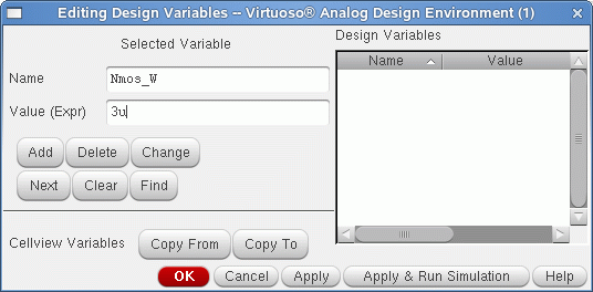
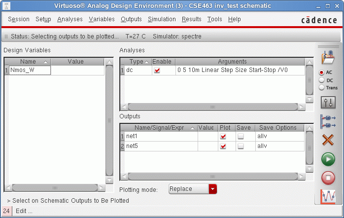
In this window, we will need to specify 3 things. First, the type of schematic analysis. We are interested in a dc analysis and we are going to sweep the V0 voltage source between 0v and 5V. Second, which nets are we going to plotted. We want to plot the input (in) and output (out) nets. And finally, the variable name which we declared earlier must be initialized. If you try to run the simulation without declaring the variable, the simulator will stop and it will enter the variable name in the simulator window automatically. It will then require you to enter a value for this variable. You can also enter yourself the variable name and value. To do so, go in Variables → Edit… in the simulator window. A selection box will prompt you for the name and the value of the variable. Enter the name of the variable and a value and press the add button.
Press OK. Once you have completed these steps, the Virtuoso Analog Design Environment window should look like as below.
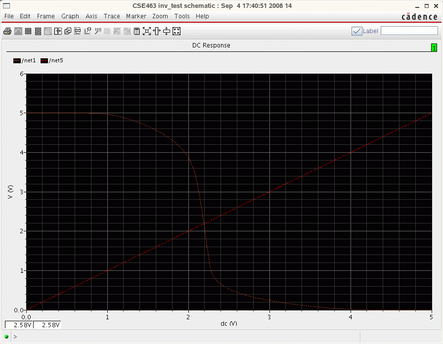
The next step is to run the simulation. Press on the "green play" button on the side of the Virtuoso Analog Design Environment window. You should see the following waveform shown below.
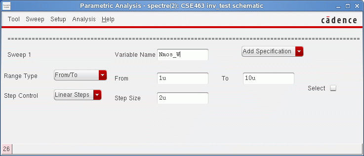
The next step is to perform a parametric sweep analysis of the inverter. We would like to sweep the width of the nmos transistor between 1um and 10um in increments of 2um. To do so, in the Virtuoso Analog Design Environment window go under Tools- >Parametric Analysis. A new window will appear. In this window we will specify the parameters we would like to sweep.
In the Variable Name box, we have entered the name of the variable Nmos_W. In the Range Type section, we have specified a sweep From: 1u To: 10u in Linear Steps increments of 2u. In this window you can add other variables if you want to sweep. You can sweep multiple parameters simultaneously if desired.
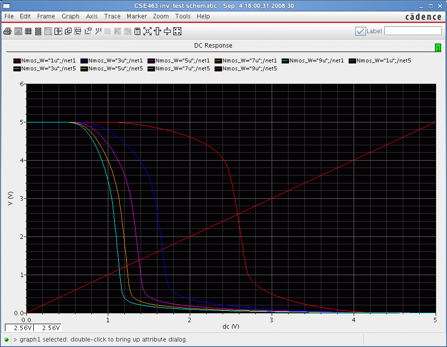
Now you are ready to run the parametric analysis. In the Parametric Analysis window, go under Analysis->Run. This will execute this analysis. The results will be plot after few seconds and they are presented below.
Both input and output waveforms are plotted on the same graph. At the top of the graph, the parameters of the different colors on the graph are explained. You can also point and select a waveform. Once selected, if you hold down the left mouse button and move the selected waveform, a text will appear describing the parameter i.e. Nmos_W value of that particular curve. You can observe that as the width of the nmos transistor is increased the Vlt value i.e. the point where Vin and Vout cross, is moved closer to ground.
Information is provided "as is" without warranty or guarantee of any kind. No statement is made and no attempt has been made to examine the information, either with respect to operability, origin, authorship, or otherwise.
Please use this information at your own risk--and any attempt to use this information is at your own risk--we recommend using it on a copy of your data to be sure you understand what it does and under what conditions. Keep your master intact until you are personally satisfied with the use of this information within your environment."
Cadence® is a trademark of Cadence Design Systems, Inc., 555 River Oaks Parkway, San Jose, CA 95134
For web related questions contact: Viktor Gruev, Michael Hall
