Difference between revisions of "Tutorials:Cadence:TransistorDCAnalysis"
(Created page with "= Schematic Simulation of Test Transistor = In the schematic of test_transistor, left click '''Editing:Launch → ADE L'''. The spectre window should appear. <img src="image...") |
|||
| Line 3: | Line 3: | ||
In the schematic of test_transistor, left click '''Editing:Launch → ADE L'''. The spectre window should appear. | In the schematic of test_transistor, left click '''Editing:Launch → ADE L'''. The spectre window should appear. | ||
| − | + | [[File:Tutorials-Cadence-Test_transistor7.gif]] | |
We want to specify the type of analysis we want to perform. We are going to select a DC analysis. Left click <strong>Analog Artist:Analyses->Choose?</strong> Click on the <strong>dc</strong> button for Analysis. Click '''Component Parameter''' button for sweep variable. In the '''Sweep Range''', fill '''0 and 5V''' for the start and stop. Left click on the '''Select Component'''. Now go back to the schematic and select the voltage source you want to sweep. Click on the vdc that is connected to the input of the inverter. This will pop-up a small window, which requests the Parameter Name. Click on '''dc''' to sweep the voltage. Go back to your Analysis Choose window, which should look like the one below, and click on OK. | We want to specify the type of analysis we want to perform. We are going to select a DC analysis. Left click <strong>Analog Artist:Analyses->Choose?</strong> Click on the <strong>dc</strong> button for Analysis. Click '''Component Parameter''' button for sweep variable. In the '''Sweep Range''', fill '''0 and 5V''' for the start and stop. Left click on the '''Select Component'''. Now go back to the schematic and select the voltage source you want to sweep. Click on the vdc that is connected to the input of the inverter. This will pop-up a small window, which requests the Parameter Name. Click on '''dc''' to sweep the voltage. Go back to your Analysis Choose window, which should look like the one below, and click on OK. | ||
Revision as of 17:17, 31 October 2010
Schematic Simulation of Test Transistor
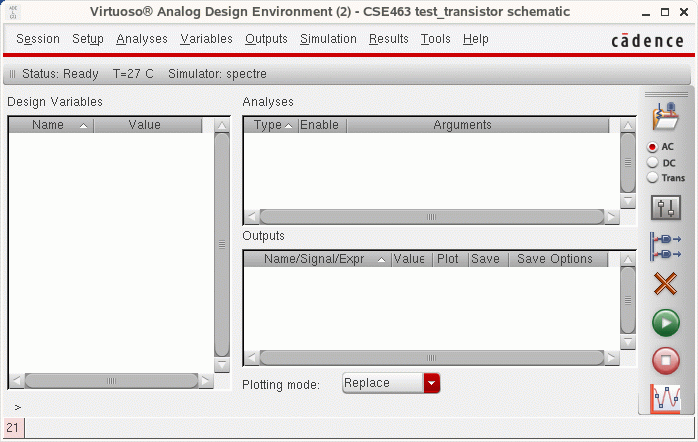
In the schematic of test_transistor, left click Editing:Launch → ADE L. The spectre window should appear.
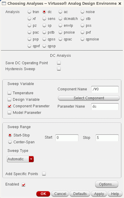
We want to specify the type of analysis we want to perform. We are going to select a DC analysis. Left click Analog Artist:Analyses->Choose? Click on the dc button for Analysis. Click Component Parameter button for sweep variable. In the Sweep Range, fill 0 and 5V for the start and stop. Left click on the Select Component. Now go back to the schematic and select the voltage source you want to sweep. Click on the vdc that is connected to the input of the inverter. This will pop-up a small window, which requests the Parameter Name. Click on dc to sweep the voltage. Go back to your Analysis Choose window, which should look like the one below, and click on OK.
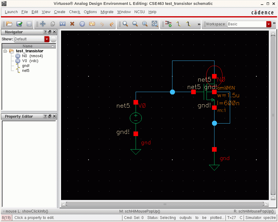
Second, we want to select which output voltages to be plotted. Left click on Analog Artist: Outputs → To be Plotted → Select on Schematic. We want to plot the drain-source current of the transistor. Click on the square of a symbol where the current is flowing through (example the square of the drain terminal of the transistor symbol). There will be a circle around the square node indicating that a current is selected. Once you have selected the current to be plotted, the schematic will look as follows:
Your Analog Environment window should appear similar to the figure bellow:
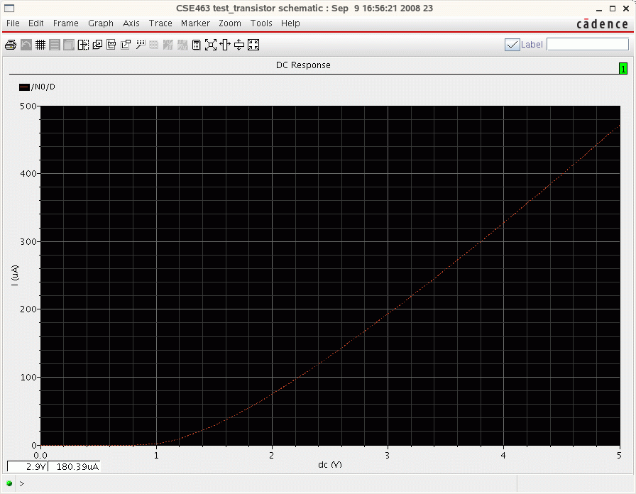
You are ready to run the simulation. Left Click Simulation → Run or click on the green play icon in the Analog Environment window. The result window, as the one below will appear shortly. Explore the pull down menus in this window in order to customize your results. For instance, left click Axes → Strip in order to separate the different curves. Press on the calculator icon. This icon will bring up a calculator and you can perform various operations on the output waveform, such as derivatives, square root, max, min, etc.
To plot the results left click Waveform Window: Window → hardcopy. Select the option to Send Plot Only to File and also don't forget to disable the header option in order not to waste paper. You might also disable Mail Log To to prevent it from mailing you about the status of printing.
Now exit the Cadence Spice. Left click on Analog Environment:Session → Quit. Remember NOT to save the current state. If you choose to save the current state, several hundreds of megabytes will be used in order to save your last simulation.
Information is provided "as is" without warranty or guarantee of any kind. No statement is made and no attempt has been made to examine the information, either with respect to operability, origin, authorship, or otherwise.
Please use this information at your own risk--and any attempt to use this information is at your own risk--we recommend using it on a copy of your data to be sure you understand what it does and under what conditions. Keep your master intact until you are personally satisfied with the use of this information within your environment."
Cadence® is a trademark of Cadence Design Systems, Inc., 555 River Oaks Parkway, San Jose, CA 95134
For web related questions contact: Viktor Gruev, Michael Hall


