Difference between revisions of "Tutorials:Cadence:LayoutDRC"
| Line 25: | Line 25: | ||
</li> | </li> | ||
</ol> | </ol> | ||
| − | + | <noinclude> | |
[[Tutorials:Cadence:CreatingLayoutInverter|Prev]] : [[Tutorials:Cadence:LayoutExtractingParasitics|Next]] : [[Tutorials:Cadence:Main|Up]] | [[Tutorials:Cadence:CreatingLayoutInverter|Prev]] : [[Tutorials:Cadence:LayoutExtractingParasitics|Next]] : [[Tutorials:Cadence:Main|Up]] | ||
| Line 32: | Line 32: | ||
---- | ---- | ||
{{Template:CadenceDisclaimer}} | {{Template:CadenceDisclaimer}} | ||
| + | </noinclude> | ||
Latest revision as of 18:56, 10 November 2010
Design Rule Check (DRC)
Our next step in the Design Process is to perform a Design Rule Check, more commonly known as DRC, on the layout. Although designers might be conscious of the design rules when performing the layout, there is a possibility of overlooking and thus violating the design rules. So, the DRC is a step taken to prompt us of any violations. This step is important because the violation of any design rules would result in a higher probability, and in some cases an absolute certainty, that the fabricated chip does not work as desired.
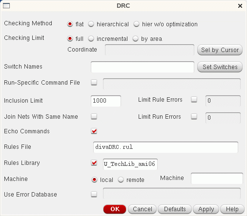
To run the DRC, choose DRC... from the Verify menu in the layout view window. A pop-up menu will appear.
You need to make sure that you're in edit mode for your layout that you want to run DRC on. For huge layouts, DRC might take a bit of time to perform. You can shorten this time by deselecting the Echo Commands option. Click on the OK button.
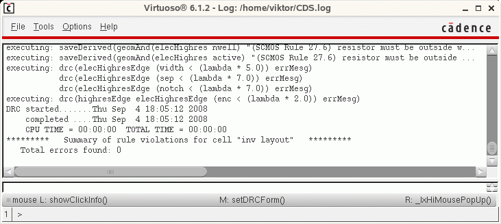
Cadence then runs the DRC and reports the errors or warnings, if any, in the CIW window.
The CIW window above shows that there are no errors or warnings found in the DRC process.
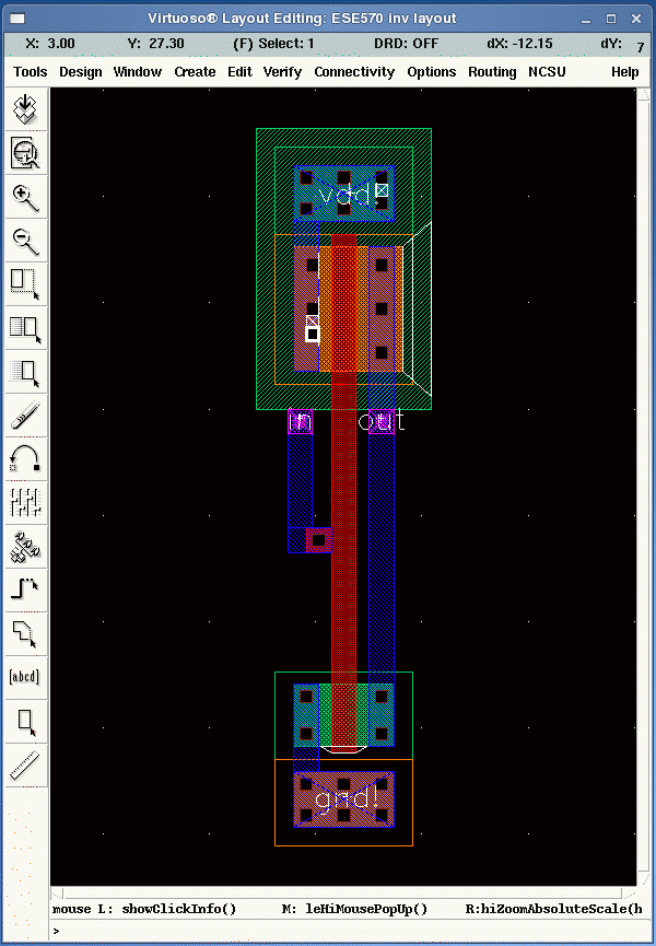
Let's perform a DRC on a layout that has errors. For the purposes of this tutorial, this step is strongly recommended so that you can gain some experience in dealing with layout DRC violations. You can purposely violate a design rule by stretching any of the mask layers to some ridiculously large dimension or by moving/shifting some layer as shown below. In this case, the pactive and cc.dg contact layers are shifted slightly to the right.
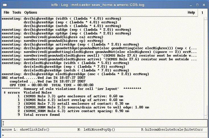
The layout above leads to the results of the DRC. Errors are indicated by markers (white as shown above) but in your layout, these markers will blink. The errors are also reported in the CIW as shown below.
- You may then proceed to correct the errors according to the design rules. Taking the above as an example, SCMOS Rule 6.2 states that the minimum spacing between active and contact layers is 0.90 um.
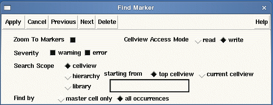
When performing huge layouts, the blinking markers might not be easily located at times. Fortunately, Cadence has an easy search tool. Under the Verify menu in the layout window, choose Markers → Find...
A pop-up menu will appear. Click on the Zoom to Markers box.
Click on the Apply button and Cadence will zoom in to the errors or warnings as desired. If there are more than one errors/warnings, as is almost always the case, you can view each one of them by clicking on Next.
Information is provided "as is" without warranty or guarantee of any kind. No statement is made and no attempt has been made to examine the information, either with respect to operability, origin, authorship, or otherwise.
Please use this information at your own risk--and any attempt to use this information is at your own risk--we recommend using it on a copy of your data to be sure you understand what it does and under what conditions. Keep your master intact until you are personally satisfied with the use of this information within your environment."
Cadence® is a trademark of Cadence Design Systems, Inc., 555 River Oaks Parkway, San Jose, CA 95134
For web related questions contact: Viktor Gruev, Michael Hall
