How to use inherited connections
Help resources
- IC-6146.14 → Virtuoso Schematic Editor → Virtuoso Schematic Editor L User Guide; → Understanding Connectivity and Naming Conventions → Inherited Connections
- IC-6146.14 → Virtuoso Layout Suite → Virtuoso Layout Suite L User Guide → Editing and Defining Properties → Using Net Expressions and Inherited Connections
Inherited connections provide a convenient way to use multiple power supplies in a design by defining a single power supply in a low-level schematic that is overridable. This can reduce the need to draw power and gnd pin connections explicitly on each symbol (useful for digital gates). In this how-to, a method for using and defining inherited connections will be given.
Note, the NCSU Design Toolkit replaces the basic library from Cadence with its own which may not have the vdd_inherit or gnd_inherit cells. To add this library to your CDS project with the name basic_cds, add the following line to the cds.lib file:
DEFINE basic_cds $IC/tools/dfII/etc/cdslib/basic
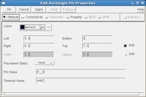
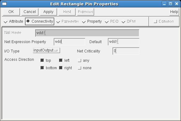
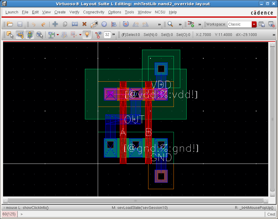
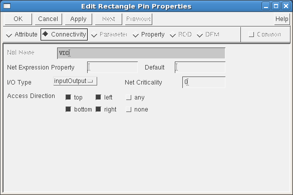
Inherited connections use Net Expressions in Cadence which provide a way of renaming a net. There are four components of a net expression (ex. [@search property name:%:default global search name]):
- search scope
- search property name
- format instruction
- default global search name - shows what the wire or pin is connected to by default
When a net expression is formed, an asterisk (*) is shown after the global name indicating that it is a net expression.
In the basic_cds library, there are four inherited supply symbols. These are given in the table below along with their associated net exprssion label:
| Inherited Supply Symbol | Net Expression Label |
|---|---|
vcc_inherit |
[@vcc:%:vcc!]
|
vdd_inherit |
[@vdd:%:vdd!]
|
gnd_inherit |
[@gnd:%:gnd!]
|
vss_inherit |
[@vss:%:vss!]
|
nand2 gate
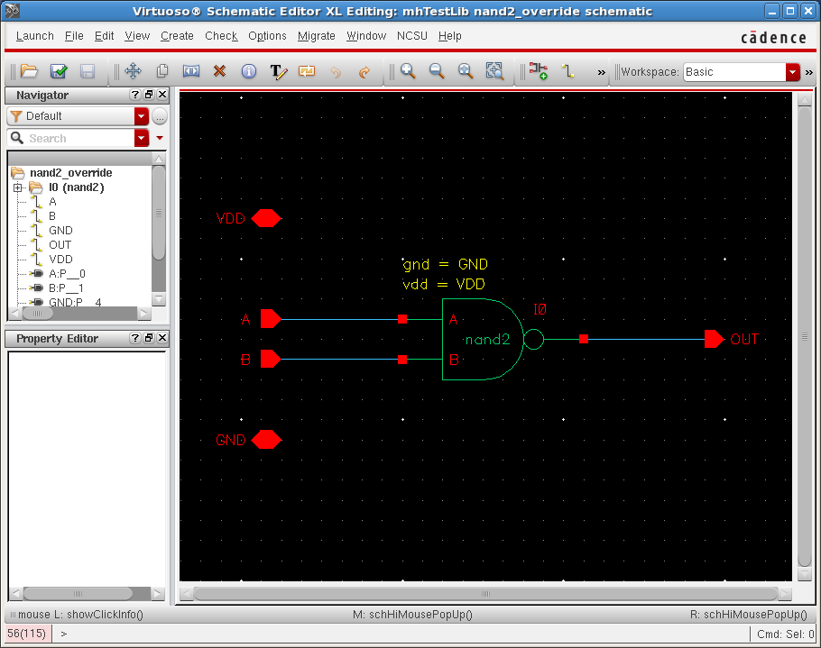
Here, is an example of using inherited connections using a 2-input NAND gate (nand2).
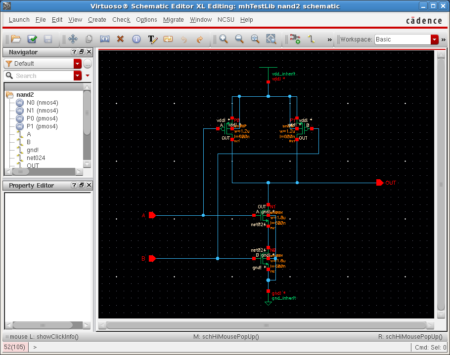
First, in the Library Manager, create a new schematic cell view using File → New → Cell View.... Then under the field Cell, type nand2. For Type select schematic. And for the View type schematic. Then draw the nand2 gate as shown below using the vdd_inherit and gnd_inherit symbols from the basic_cds library.
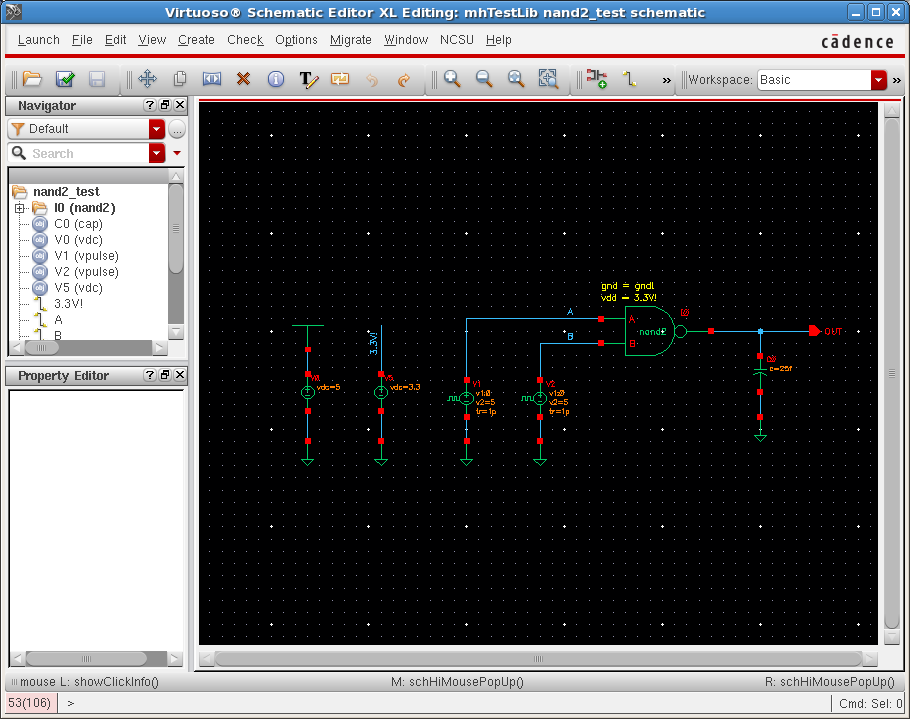
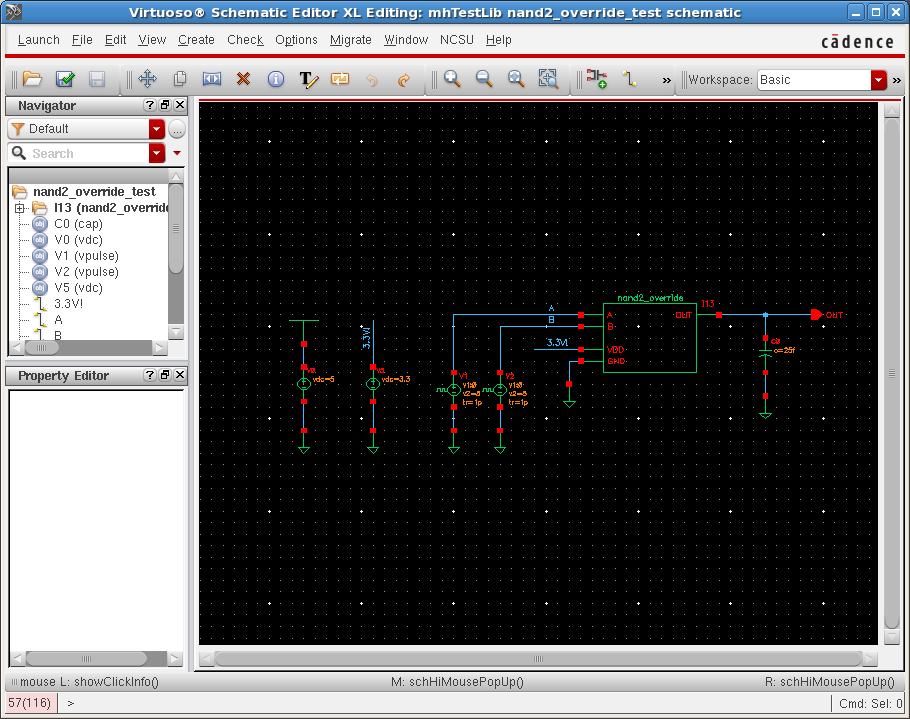
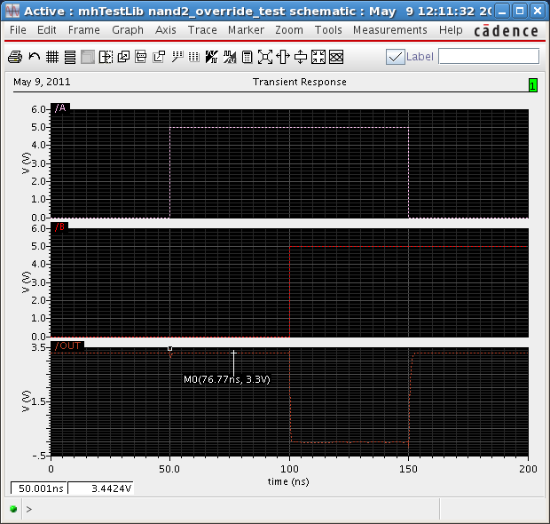
Next, create a test schematic for the nand2 gate called nand2_test. This test schematic is designed to override the power supply nets by using Net Expressions. The overrides are shown in yellow on the schematic. The global vdd! net is set to 5V and the vdd power supply of the nand2 gate is set to 3.3V!:
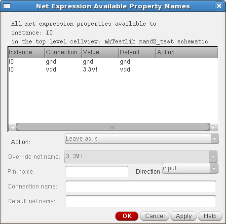
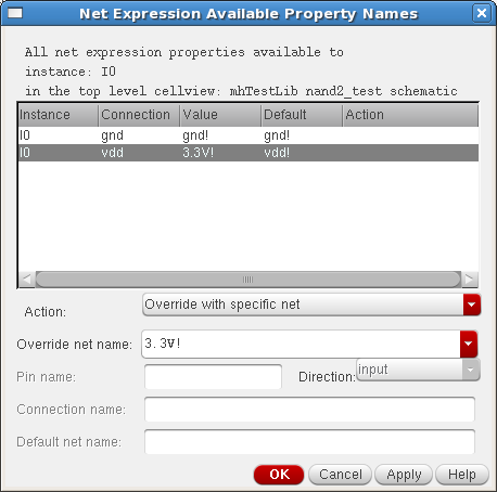
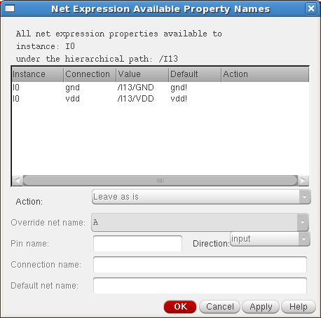
The Net Expressions can be set by
