Tutorials:Cadence:LayoutExtractingParasitics
Layout: Extracting Parasitics
A successful DRC ensures that the layout passes through the rules designed for faultless fabrication. However, it does not guarantee if it really represents the circuit you desire to fabricate. In our case, for an inverter, we really need a tool than can compare the connectivities of our layout with that of the schematic and ensure that it is really a layout for an inverter. One way Cadence does this is by generating an Hspice netlist file from the layout and comparing it with the netlist for the schematic. This is the essence of the LVS tool. Before performing an LVS, the layout has to be extracted.
-
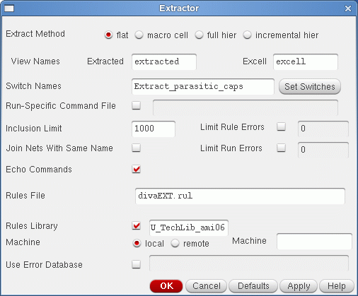
The first step is to extract all the connectivities and parasitic capacitances from your layout design. From the layout view window, choose Extract... under the Verify menu. A window will pop-up. Make sure that the entries are as given below. For the entry in Switch Names, click on Set Switches. A window will pop-up. Choose the option for Extract_parasitic_caps. Note that, if for some reason, you did not want to extract the parasitic capacitances, you would leave the Switch Names empty. Finally, click on OK. The beauty of this extraction tool is that Cadence will recognize not only all the connections but also more importantly, if you have designed the layout correctly, it will also recognize all the nmos and pmos transistors.
Make sure that your layout window is in Edit mode.
-
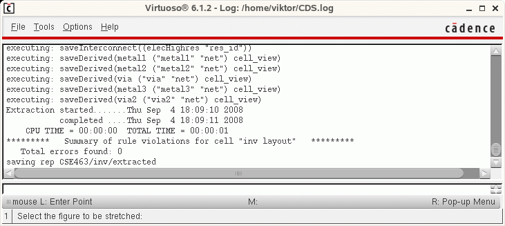
Your layout will then be extracted and while Cadence is doing so, the intermediary steps will be displayed in the CIW. It will tell you whether the extraction is successful or not.

