Tutorials:Cadence:LayoutSimulation
Post Layout Simulation
The parasitic capacitances extracted according to how your layout is designed might be critical in affecting the actual performance of your design. In order to get an idea of how the design would work from your layout, you should perform a post-layout simulation from the extracted view. The procedure is identical to that for simulating from the schematic view.
Our main goal here is to obtain the netlist of the layout design from Cadence in the Spectre format so that we can run a Spectre simulation from the LINUX prompt. This method is preferable for CSE463 students and people who like to write and edit the Spectre code themselves. However, for all others you may as well want to use the complete Affirma Analog Environment simulation tools to perform your simulations.
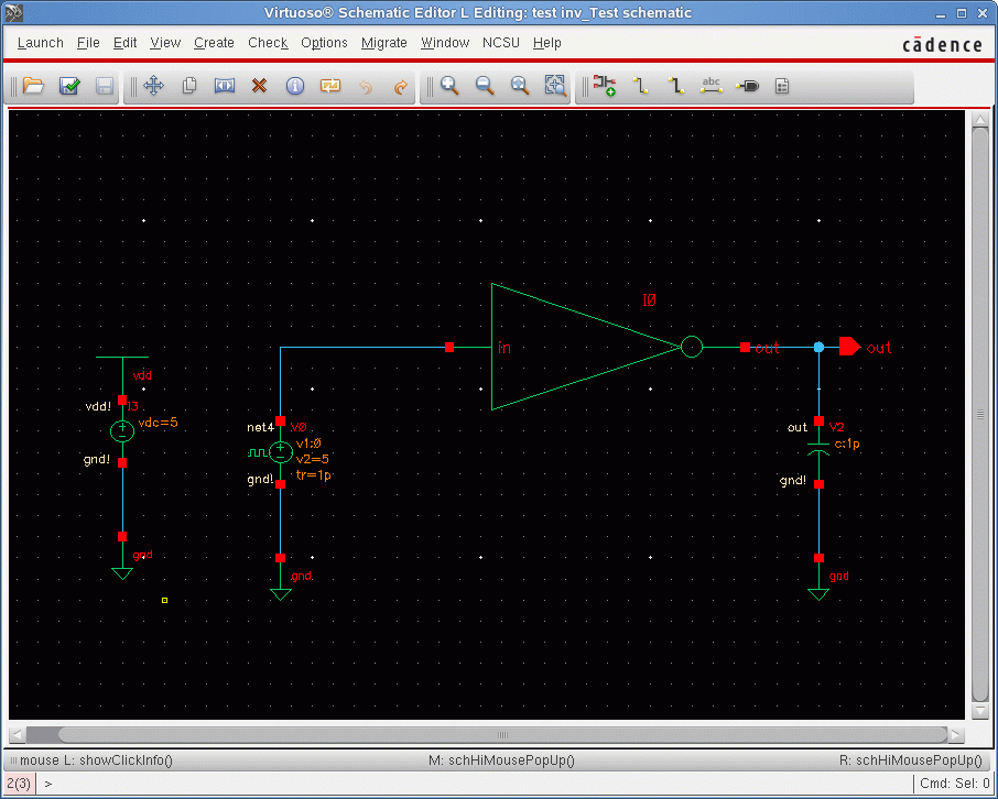
Open up the test schematic for the inverter in edit mode. You will see the following window:
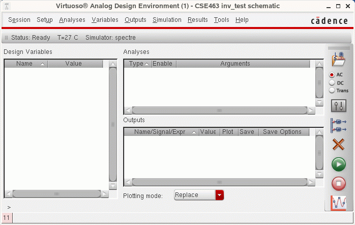
Under the Launch menu, choose ADE L. A window similar to the one shown below will pop-up.
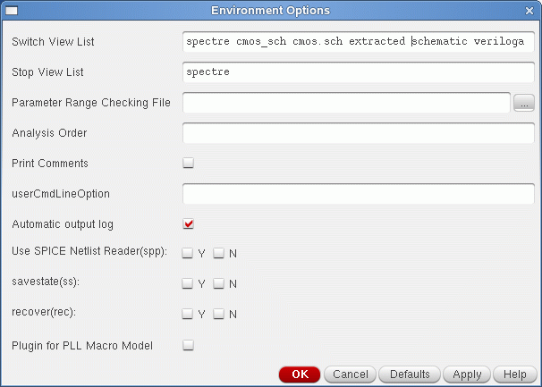
Click on Setup → Environment… and you will see the Environment Options window open up. Originally, the Switch View List should contain the following items:
spectre cmos_sch cmos.sch schematic veriloga ahdl
In order for Cadence to simulate through the extracted view of the layout design instead of the schematic view, you will include an additional item (extracted) in the Switch View List such that it now contains the following:
spectre cmos_sch cmos.sch extracted schematic veriloga ahdl
The Enviroment Options window should look like the one bellow:
Press OK. You can now perform the simulation in the same manner as before using ADL Spectre methods. This additional step allows you to take into account all the parasitic capacitances (eg. from interconnects and source/drain areas) that were extracted into the extraction view from your layout design. You may be able to notice subtle differences in the post-layout simulation results or waveforms as compared to the pre-layout schematic view results.
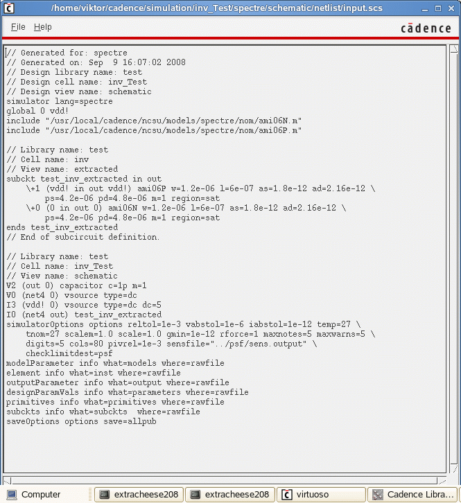
To be absolutely sure that Cadence is running simulations through the extracted view, you can view the generated a netlist by clicking on Simulation → Netlist → Create … from the Analog Environment Simulation window. The generated netlist will open up in another window. Within the first 20 or so lines, you should be able to search for a single line of code that confirms that the extracted view was indeed taken. This line of code should look something like the following:
// Library name: test
// Cell name: inv
// View name: extracted
The last line points to the file which will be used for simulation. In this case the extracted view of cell name inverter will be used.
Information is provided "as is" without warranty or guarantee of any kind. No statement is made and no attempt has been made to examine the information, either with respect to operability, origin, authorship, or otherwise.
Please use this information at your own risk--and any attempt to use this information is at your own risk--we recommend using it on a copy of your data to be sure you understand what it does and under what conditions. Keep your master intact until you are personally satisfied with the use of this information within your environment."
Cadence® is a trademark of Cadence Design Systems, Inc., 555 River Oaks Parkway, San Jose, CA 95134
For web related questions contact: Viktor Gruev, Michael Hall


