Tutorials:Cadence:CreatingSymbolInverter
Creating Symbols: Inverter Symbol
The symbol editor lets you create a "black box" description of a cell using labels, pins, shapes, notes, and a selection box. Symbols make your design more readable, as you can use them in more complex designs, instead of individual transistors.
There are two different ways you can create a symbol: create a new symbol cell view using the Library Manager, or generate a symbol cell view from the schematic. Both of these ways are explained in the sub-sections below:
Create a blank symbol cell view
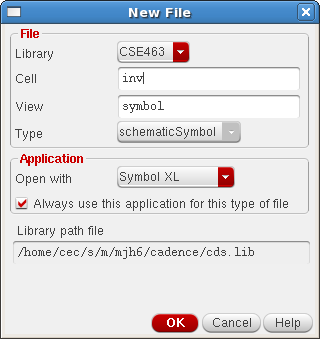
In the Library Manager click once on the CSE463 library to select this library. Then left click Library Manager: File → New → Cell View. In the Cell field type inv and in the View field type symbol. You can also click on the Type box and select schematicSymbol and the View field will be automatically filled.
Left click OK.
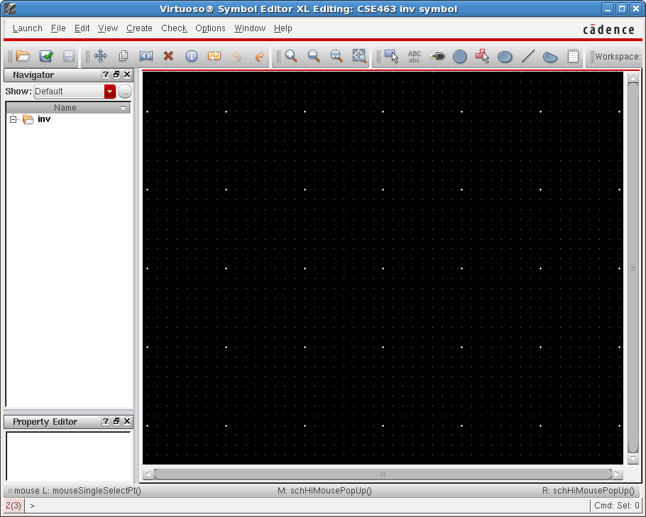
The Virtuoso Symbol Editor window like the one below should appear.
You are ready to draw a symbol for the inverter. First, we will draw a triangle to represent the inverter body. Left click Schematic Editor: Create → Shape → Polygon.
The Add Symbol Shape window appears. Left click Hide for now. To draw a polygon, click at a start point, and then click at the corners of the shape you want to create. To finish the polygon, click again on the start point. Since we are drawing an inverter, we need a sideways triangle, so make one of those. Look at the final picture at the bottom for guidance to draw.
The inverter needs a negation circle at the sideways corner of the triangle, so left click Schematic Editor: Create → Shape → Circle. Hide the Add Symbol Shape window again. Left click at the point you want to be the center of the circle. Move the mouse until the circle is the size you want, and left click again.
Now draw a line that starts at the middle of the vertical line of the triangle and ends somewhere to it's left (about 2 grid line spaces) and another line from the rightmost part of the circle to somewhere equally to the right (again about 2 grid line spaces), so left click Schematic Editor: Create → Shape → Line.
Hint: Rather than invoking the Add Symbol Shape box every time and having to go through the menus, you can use the shortcut buttons located at the top of the window.
Now, you want to add pins to the symbol. Left click Schematic Editor: Create → Pin (bindkey <p>).
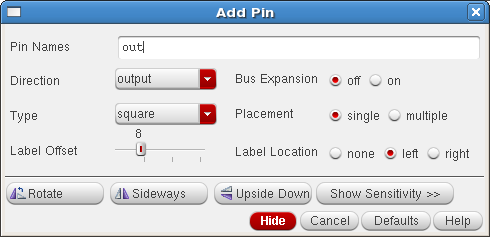
In the Pin Names box type the following pin names: in. Change the direction of the pins to input for in and output for out. Also set the Type to square, and the Label Offset to 8.
You are going to start placing the pins in the symbol. The pin looks a little different than the ones in the schematic, so be careful. You will notice that it is a box with the pin name label positioned about 2 grid line spacings away. The end of the line will have the pin name. The box is the actual pin, so it must point AWAY from the rest of the symbol.
Add the in pin on the left of the symbol. The pins in ALL cell views of a single cell must have the same attributes and names. In other words, if the type of the pin is input in the schematic, it should be input type in the symbol also. When you save your symbol, any differences between the pins of the symbol and the pins of the schematic will be reported as warnings. Following these warnings you can figure out where the inconsistency in the design has occurred.
Repeat the same procedure for the out pin. The Add Pin selection box should look like the one below:
Add the out pin on the right of the symbol.
Once you place the pins, the pin names may be hard to read for a variety of reasons. You can therefore move the pin name by clicking on the pin text label and then left click on Schematic Editor: Edit → Move (bindkey <m>). Now you can move the label and place where ever you want to. Next we want to add a label to the symbol. Left click Schematic Editor: Create → Label (bindkey <L>). The Add Symbol Label dialog box should appear.
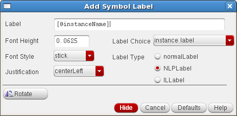
We will add an instance label. Make sure the Label Choice is set to "instance label" and change the Justification to "centerLeft". Then left click the Hide button, and place the label somewhere near the symbol of the inverter.
Later, when you use symbols to build schematic, the software needs to know which symbol is which. It does this by looking at the instance label to see which one of those it is. If you put multiple symbols into a schematic window, they will be labeled U1, U2, etc.
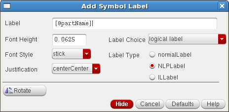
Next, we will add a logical label to the symbol which will describe the circuitry. Choose "logical label" for the Label Choice and change the Justification to "centerCenter". In this case, the label will be [@PartName]. This is a placeholder for the logical name of the inverter cell. When the inverter is later instantiated, the symbol will show the inverter cell name, inv, in place of this logical label. The Add Symbol Label window shown in the figure below:
We will add the label in the symbol. Just left click the Hide button, and place the label somewhere near the symbol of the inverter.
Next, we will add a selection box. This will tell the software how much of the symbol is actually used.
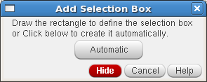
Left click Schematic Editor: Create → Selection Box...
Left click the Automatic button.
Last, we will set the origin point in the symbol. The origin point corresponds to the location of the mouse relative to the symbol when the cell is instantiated. We will set this point to the lower left corner of the selection box. Click Schematic Editor: Edit → Origin. Then left click on the lower left corner of the selection box to set the origin point.
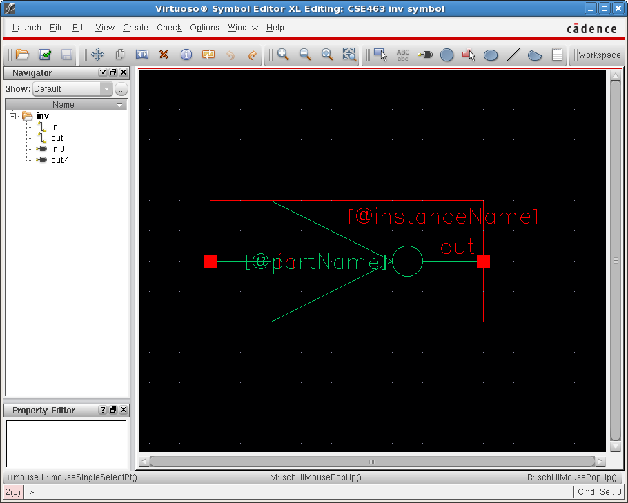
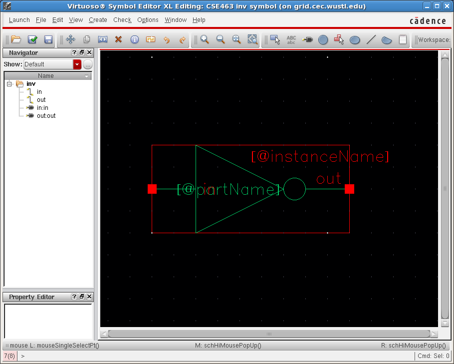
The symbol is now finished and you can save it by left clicking Schematic Editor: File → Check & Save (F8). The symbol should look like the one below.
Generate symbol from schematic
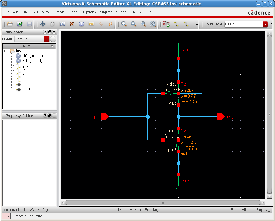
In the Library Manager click once on the CSE463 library to select this library. Then left click the inv cell and finally the schematic cell view. Right click on the schematic cell view and click Open or double click on schematic to open the schematic editor. This will give the figure shown below.
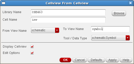
Left click Schematic Editor: Create → Cellview → From Cellview... This will then show the Cellview From Cellview window below. This window allows a symbol to be generated from the schematic view. It does this by identifying the pins that are already defined in the schematic and automatically generating a symbol with the same pins.
Click OK.
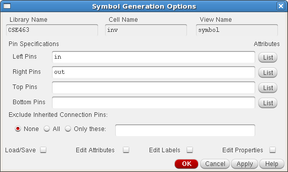
Next, the Symbol Generation Options window will appear which will list the pin specifications of the new symbol. Cadence has already identified the input and output pins and has automatically added the input pin, in, to the left pins and the output pin, out, to the right pins. The Symbol Generation Options window is shown below.
Click OK.
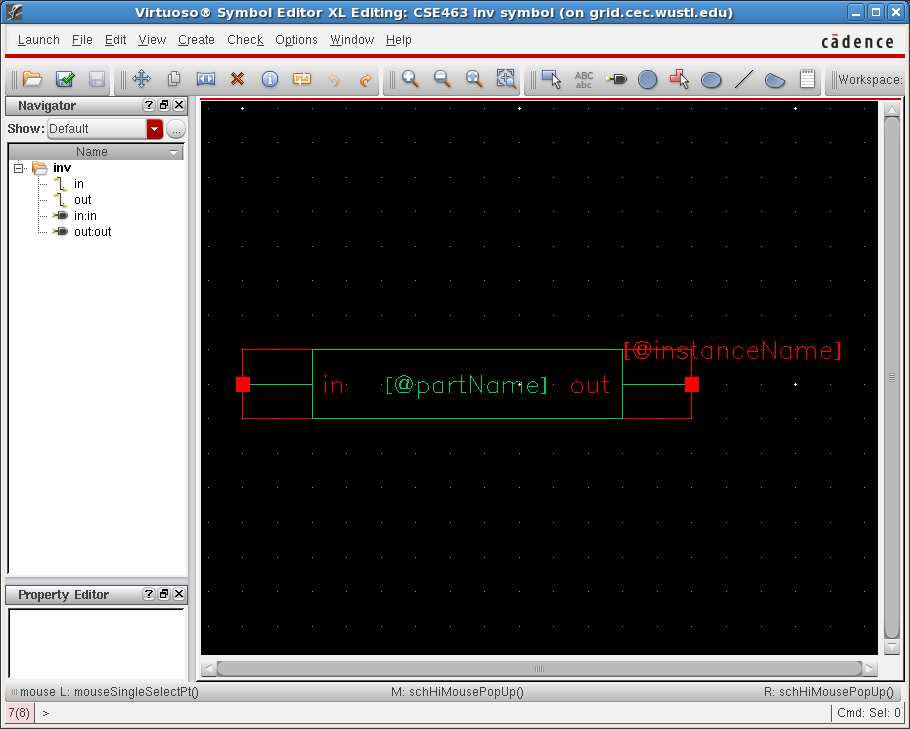
Cadence has now generated a default symbol using the pin specifications previously given. You can now use this symbol as a starting point to create the inverter symbol.
First, we will draw a triangle to represent the inverter body. Left click Schematic Editor: Create → Shape → Polygon.
The Add Symbol Shape window appears. Left click Hide for now. To draw a polygon, click at a start point, and then click at the corners of the shape you want to create. To finish the polygon, click again on the start point. Since we are drawing an inverter, we need a sideways triangle, so make one of those. Look at the final picture at the bottom for guidance to draw.
The inverter needs a negation circle at the sideways corner of the triangle, so left click Schematic Editor: Create → Shape → Circle. Hide the Add Symbol Shape window again. Left click at the point you want to be the center of the circle. Move the mouse until the circle is the size you want, and left click again.
Hint: Rather than invoking the Add Symbol Shape box every time and having to go through the menus, you can use the shortcut buttons located at the top of the window.
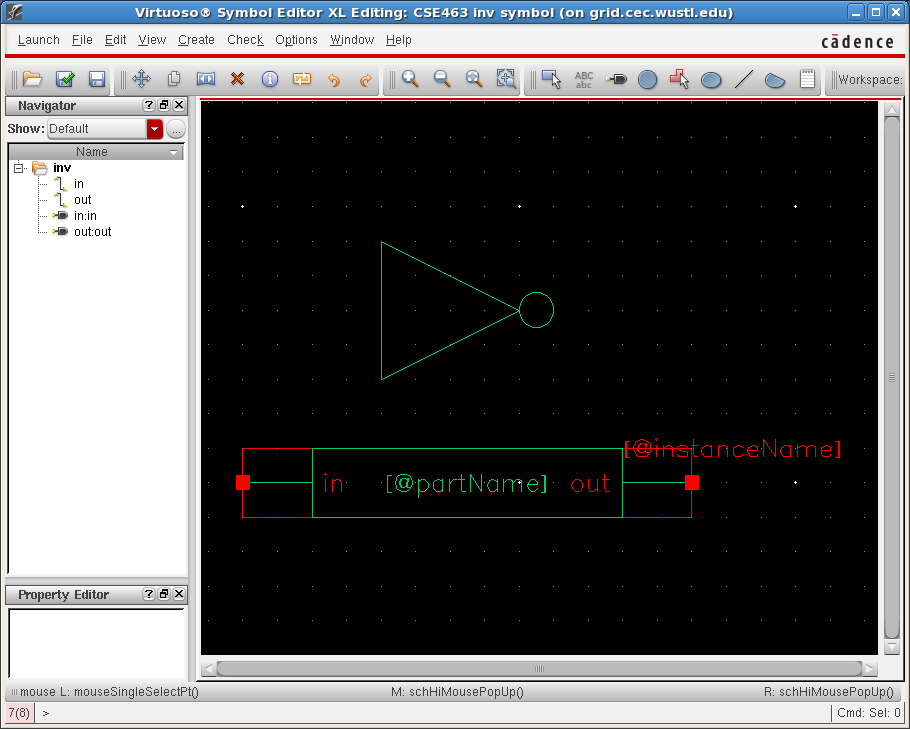
You should have a symbol that currently looks like the one below:
Next, you can move the each pin (along with the line connected to each pin) from the default symbol to the inverter symbol. Left click on Schematic Editor: Edit → Move (bindkey <m>). Now you can move the in pin to the left of the inverter symbol and the out pin to the right of the inverter symbol. You may also want to move the pin name labels to more suitable locations as necessary so that they are easy to see.
Next, move the [@instanceName] label from the default symbol to the inverter symbol positioned to the upper right (note, this label is by default centerLeft justified). Also move the [@partName] label and position it in the center of the inverter (note, this label is by default centerCenter justified). Last, move the red selection box to the inverter symbol. The selection box will need to be resized so that it fits around the inverter symbol. This is done by left clicking Schematic Editor: Edit → Stretch (bindkey <s>). The selection box will tell the software how much of the symbol is actually used.
Now, delete the rest of the default symbol by left clicking Schematic Editor: Edit → Delete (bindkey <del>) and clicking on the objects to delete.
Last, we will set the origin point in the symbol. The origin point corresponds to the location of the mouse relative to the symbol when the cell is instantiated. We will set this point to the lower left corner of the selection box. Click Schematic Editor: Edit → Origin. Then left click on the lower left corner of the selection box to set the origin point.
The symbol is now finished and you can save it by left clicking Schematic Editor: File → Check & Save (F8). The symbol should look like the one below.
Information is provided "as is" without warranty or guarantee of any kind. No statement is made and no attempt has been made to examine the information, either with respect to operability, origin, authorship, or otherwise.
Please use this information at your own risk--and any attempt to use this information is at your own risk--we recommend using it on a copy of your data to be sure you understand what it does and under what conditions. Keep your master intact until you are personally satisfied with the use of this information within your environment."
Cadence® is a trademark of Cadence Design Systems, Inc., 555 River Oaks Parkway, San Jose, CA 95134
For web related questions contact: Viktor Gruev, Michael Hall
