Tutorials:Cadence:AdvancedTopics
Advanced Topics
Pad frame
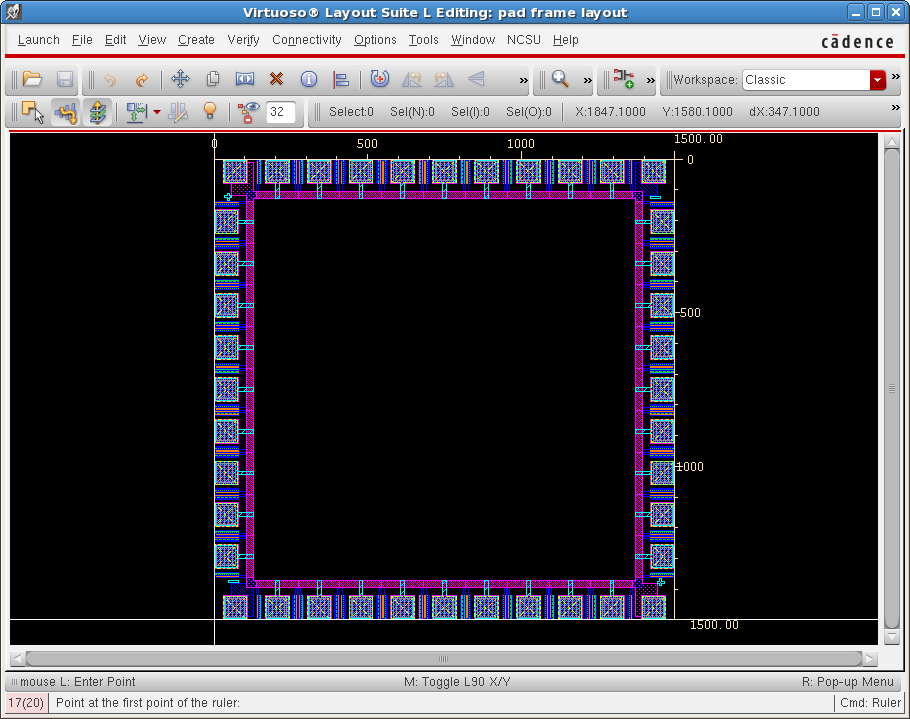
One tiny chip unit is 1.5mm x 1.5mm. The pad frame provided here has a total of 40 pins. The 4 corner pins are used for VDD and GND (note the +/- symbols in the layout) and the remaining 36 pins are available for I/O.
To use the pad frame, please do the following steps:
- Download Padframe_C5N.tgz into $HOME/cadence/library.
- Type "cd $HOME/cadence/library".
- Type "tar -xzvf Padframe_C5N.tgz". This will extract the pad library.
- Type "cd ..".
-
Edit cds.lib and add the following line:
DEFINE pad library/pad
- Execute virtuoso. The pad library will now appear in the Library Manager.
The pad frame layout is shown below.
Vector File Simulation
Now we are introducing a new simulation method under Cadence Spectre Simulator: Using Vector File. Vector file is a very convenient way to do large scale digital simulation, the manual for how to write digital vector file can be download from here:
In Cadence, first we create a NAND2 cell schematic view:
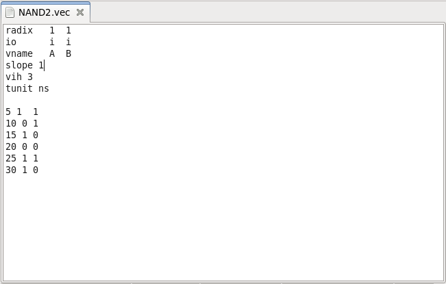
In this NAND2, we have two input ports: A and B, one output ports: C. Then in vector file, we assign values to A and B. The example vector file NAND2.vec:
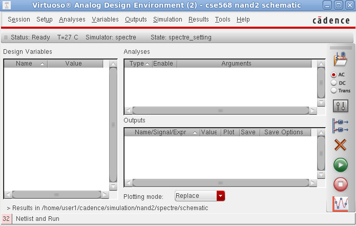
In a basic vector file, you need define the radix, i/o, tunit, and value for the input or output ports, moreover, you can also define your rise/fall time, high/low voltage. Next, we open the Cadence ADE L:
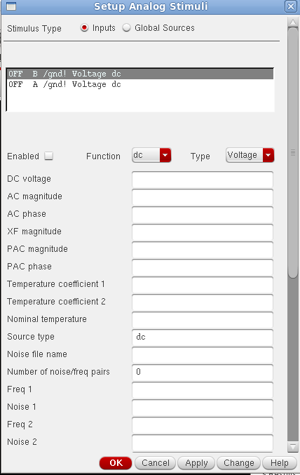
Then left click Setup->stimuli..., the window of stimuli will jump out:
Then left click to select the Globe Sources at the first row, then select vdd!, click select enable, fill the DC voltage with a value, here we just define it 3V, (Note: by giving the value to vdd! here, we don't need to load vdc module anymore), then click apply:
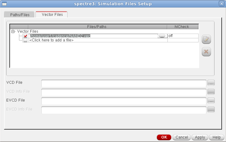
After we click OK, the window will disappear, we left click Setup-> Simulation Files, then select "Vector Files" tab at the top row, add NAND.vec as the Vector Files:
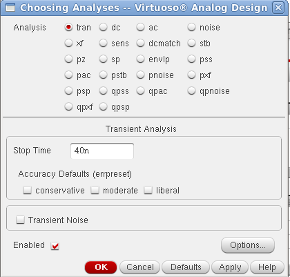
Click OK, then left click choose Analyses-> Choose..., on the "Choosing Analyses" tab, select tran, then fill the stop time with a value, here we fill it as 40n s:
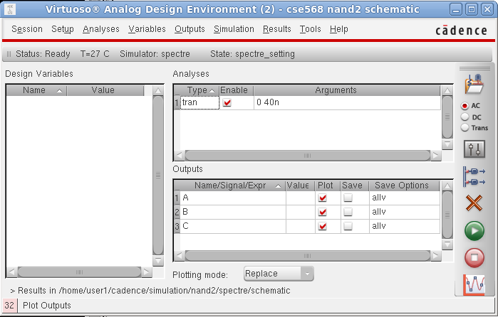
Click OK, then select the ports you want to view in the schematic by using Outputs-> To Be Plotted-> Select On Schematic, then click Netlist and Run button:
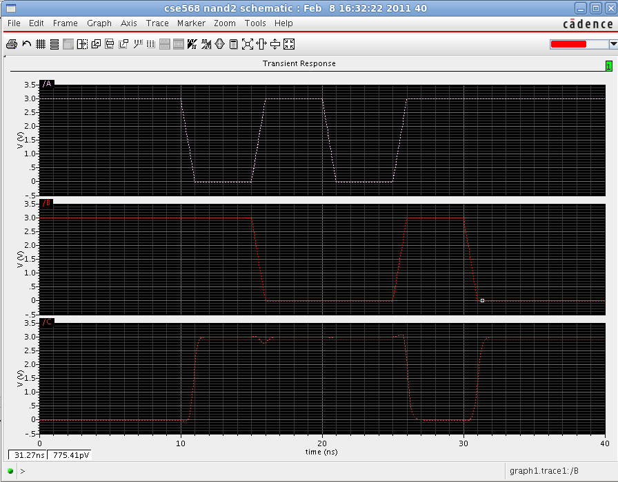
Finally, we get the waveform of this NAND2 gate:
Information is provided "as is" without warranty or guarantee of any kind. No statement is made and no attempt has been made to examine the information, either with respect to operability, origin, authorship, or otherwise.
Please use this information at your own risk--and any attempt to use this information is at your own risk--we recommend using it on a copy of your data to be sure you understand what it does and under what conditions. Keep your master intact until you are personally satisfied with the use of this information within your environment."
Cadence® is a trademark of Cadence Design Systems, Inc., 555 River Oaks Parkway, San Jose, CA 95134
For web related questions contact: Viktor Gruev, Michael Hall
