Tutorials:Cadence:SchematicSimulationTransient
Schematic Simulation: Transient Analysis of The Inverter
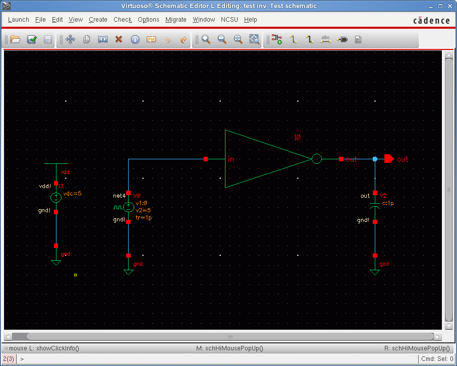
Bring up the schematic of inv_test. We need to replace the dc voltage input source with a pulse source. Click on the vdc source that is connected to the input of the inverter. The vdc should have a yellow box around it. Go to Editing: Edit → Delete or press the Del button.
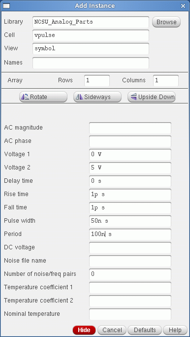
Left Click Add → Instance and select Cell Name: vpulse from Library Name: NCSU_Analog_Parts and View Name:symbol. Fill the rest of the boxes as shown in the figure below. The input pulse that we have specified is bounded between 0 and 5V. It has an initial delay of 1ns, rise and fall time of 1ps and high/low duration of 2ns.
Place this symbol such that the positive end is connected to the input of the inverter.
Save the schematic. Left Click Editing:File → Save. After we have made these changes we are ready to run a transient analysis on the inverter.
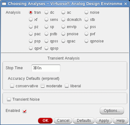
Left Click Editing:Launch → ADE L. In the Analog artist window go to Analysis → Choose... Set the transient analysis with Stop Time as 8n. We have specified a transient analysis from 0 to 300ns.
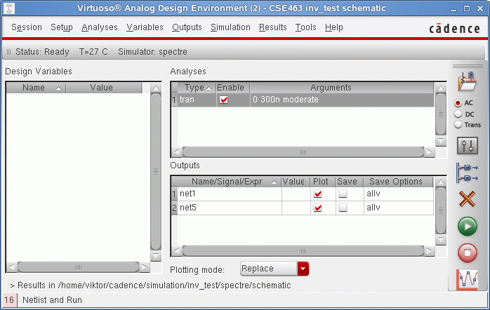
Left Click Analog Artist: Outputs → To be Plotted → Select on Schematic. Select the input and output of the inverter. Refer to the previous section, DC analysis, for the necessary steps. The analogArtist window should look like the one below.
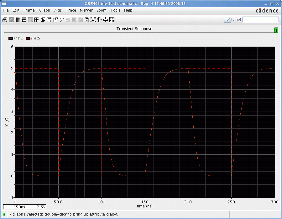
Run the simulation by pressing on the green traffic light icon. After few seconds you should be able to see the results of the transient analyses like the ones below.
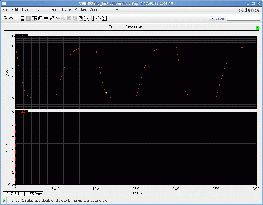
Left click Axes → Strip in order to separate the different curves. The result should look like the one bellow:
Information is provided "as is" without warranty or guarantee of any kind. No statement is made and no attempt has been made to examine the information, either with respect to operability, origin, authorship, or otherwise.
Please use this information at your own risk--and any attempt to use this information is at your own risk--we recommend using it on a copy of your data to be sure you understand what it does and under what conditions. Keep your master intact until you are personally satisfied with the use of this information within your environment."
Cadence® is a trademark of Cadence Design Systems, Inc., 555 River Oaks Parkway, San Jose, CA 95134
For web related questions contact: Viktor Gruev, Michael Hall
