Tutorials:Cadence:TransistorDCAnalysis
Schematic Simulation of Test Transistor
In the schematic of test_transistor, left click Schematic Editor: Launch → ADE L. The Spectre window should appear.
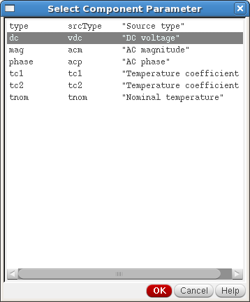
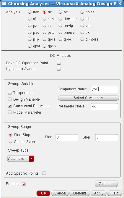
We want to specify the type of analysis we want to perform. We are going to select a DC analysis. Left click Analog Artist: Analyses → Choose.... Click on the dc button for Analysis. Left click Component Parameter button for under Sweep Variable. In the Sweep Range, fill 0 and 5V for the Start and Stop. Left click on the Select Component. Now go back to the schematic and select the voltage source you want to sweep. Click on the vdc that is connected to the input of the inverter. This will pop-up the Select Component Parameter form shown below, which requests the selection for the Parameter Name.
Left click on dc to sweep the voltage and then click OK to go back to your Analysis Choose window, which should look like the one below.
Left click OK.
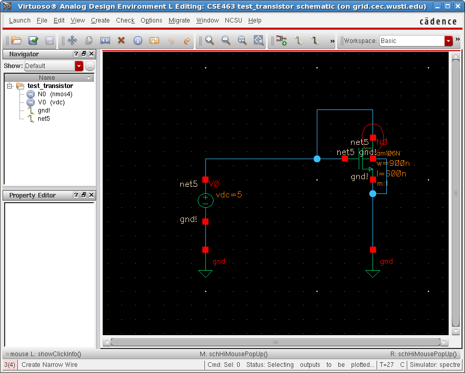
Second, we want to select which output voltages to be plotted. Left click on Analog Artist: Outputs → To Be Plotted → Select On Schematic. We want to plot the drain-source current of the transistor. Click on the square of a symbol where the current is flowing through (in this example, the square of the drain terminal of the transistor symbol). There will be a circle around the square node indicating that a current is selected. Once you have selected the current to be plotted, the schematic will look as follows:
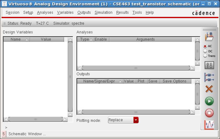
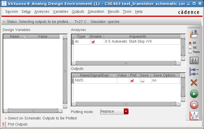
Your Analog Design Environment window should appear similar to the figure below:
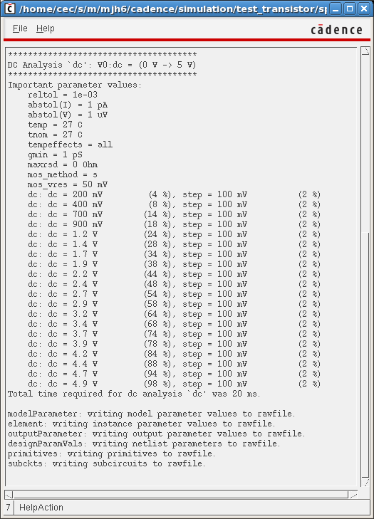
You are ready to run the simulation. Left click Simulation → Run or click on the green play icon in the Analog Design Environment window. The Spectre output window appears as shown below, followed immediately by the Waveform window:
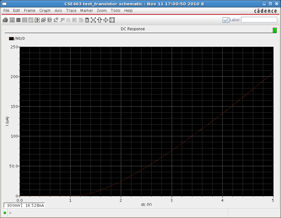
The results appear in the Waveform window, as shown below:
Explore the pull down menus in this window in order to customize your results. For instance, left click Axes → Strip in order to separate multiple curves (you must have more than one output selected for plotting for this to be available). Press on the calculator icon. This icon will bring up a calculator and you can perform various operations on the output waveform, such as derivatives, square root, max, min, etc.
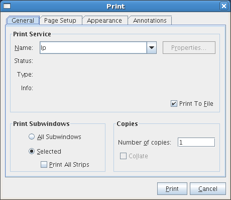
To plot the results left click Waveform Window: File → Print.
Select the option to Print To File to save it as Post Script. Left click Print.
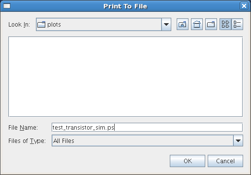
Create a directory named plots. Then type a name for the Post Script file and left click OK. A plot of the waveform is now created. Note, this can be converted to PDF using the UNIX command ps2pdf.
Now exit the Cadence Spice. Left click on Analog Artist: Session → Quit. Cadence will ask whether or not you want to save the current state as shown below:
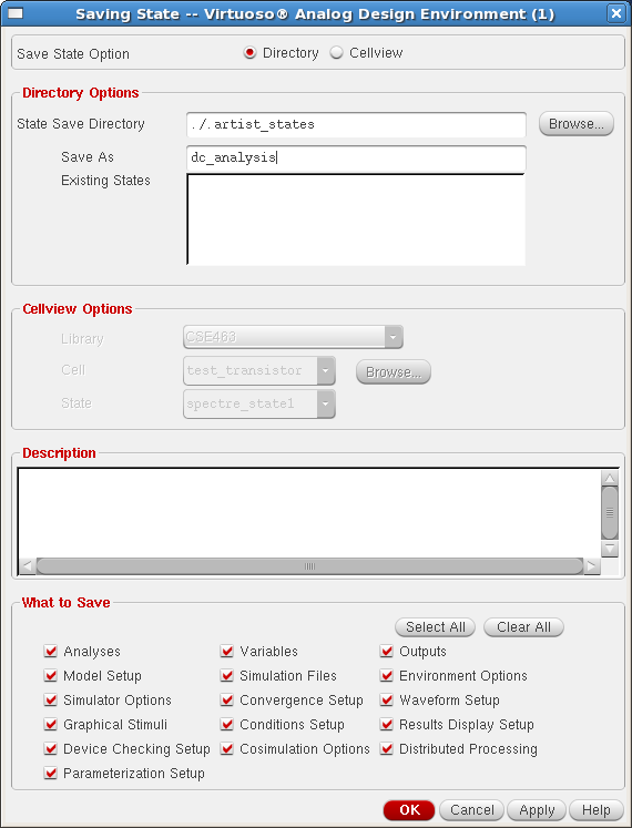
If you choose Yes to save the current state, the Saving State form will appear:
Type a name for the state in the Save As field and left click OK.
Information is provided "as is" without warranty or guarantee of any kind. No statement is made and no attempt has been made to examine the information, either with respect to operability, origin, authorship, or otherwise.
Please use this information at your own risk--and any attempt to use this information is at your own risk--we recommend using it on a copy of your data to be sure you understand what it does and under what conditions. Keep your master intact until you are personally satisfied with the use of this information within your environment."
Cadence® is a trademark of Cadence Design Systems, Inc., 555 River Oaks Parkway, San Jose, CA 95134
For web related questions contact: Viktor Gruev, Michael Hall
